

 Search


1 / 1
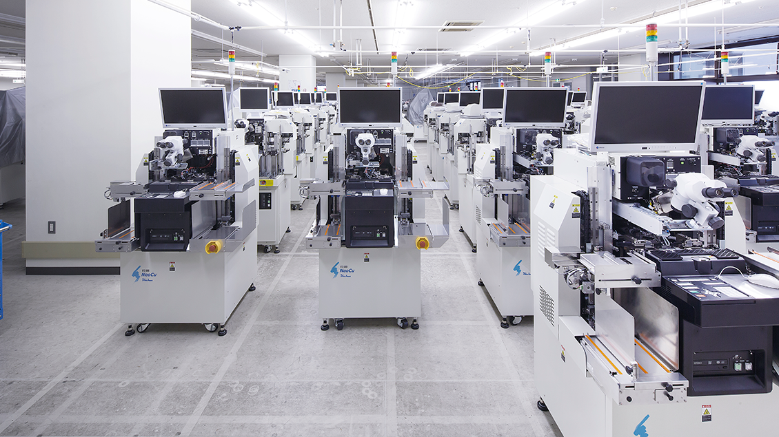
Ultra High Speed C4/C2 Flip Chip Bonder

Price:
price negotiable
Brand Name:
SHINKAWA LTD.Country Region:
JapanModel No:
YSB55w
 Post Requirements
SHINKAWA LTD. 
Country: Japan
Main Products: Wire Bonder、Die Bonder
View more
Price:
price negotiable
Brand Name:
SHINKAWA LTD.Country Region:
JapanModel No:
YSB55w
 Post Requirements
SHINKAWA LTD. 
Japan
Main Products:
Wire Bonder、Die Bonder
Product information
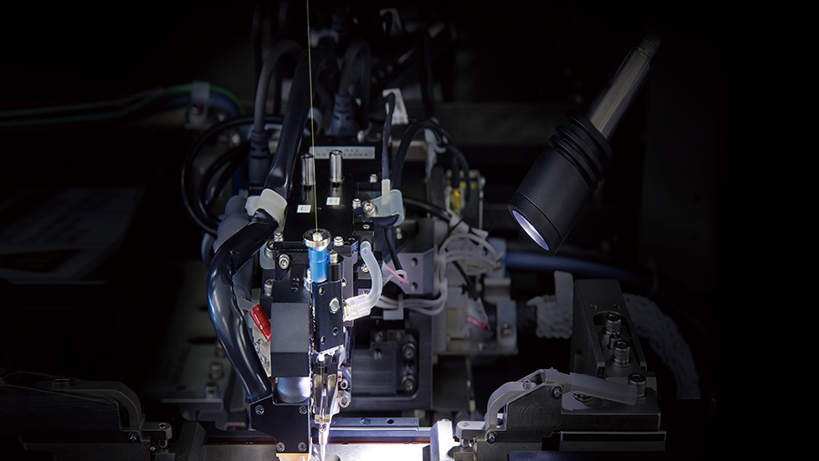
- 实现超过以往机型约3倍的生产率与约2倍的高精度贴装。在不断扩大的倒装芯片市场掀起“半导体组装革命”。
- 可同时高速吸附8个元件并同时高速浸焊,使贴装能力达到13,000UPH
- 高精度 ±5µm(3σ)
- 高品质、通用性强
- 双倒装机头可实现并行工作以及8个芯片的高速同时贴片
- 高刚性框架和控制演算法赋予产品极佳的定位精度
- 搭载可补正Bump位置的高性能摄像机
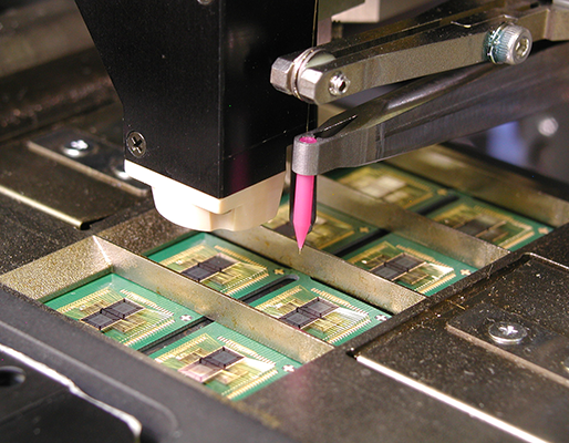
- 可对应□2~□30mm之间的多种芯片尺寸
- 可简单更改设定助焊剂的浸胶机构
基本规格
| 项目 | 内容 |
|---|---|
| 型式 | YSB55w |
| 対象基板 | L240×W200~L50×W50mm |
| 基板厚度 | 0.2~3.0mm |
| 传送方向 | 左→右(选购品:右→左传送) |
| 贴装精度 | ±5µm(3σ) |
| 贴装能力 | 13,000UPH(包含实际生产流程时间的最佳条件下) |
| 元件供给形态 | 12英寸晶片 |
| 对象元件 | □2~30mm |
| 电源规格 | 三相AC 200/208/220/240/380/400/416V ±10% 50/60Hz |
| 供给气源 | 0.45MPa以上 |
| 外形尺寸 | L2,090×D1,866×H1,550mm(安装晶片供给装置时) |
| 重量 | 约3,500kg (安装晶片供给装置时) |
※ 因改良需要,规格及外观可能会有所变更,恕不另行通知。


All products in the store
High Speed Au Wire Bonder for LED and discrete
TCB Flip Chip Bonder for Chip to Substrate
High-Accuracy Die Bonder with Advanced Pick-Up
Wide-area Adaptive High-speed Wafer Bump Bonder
Dual TCB Flip Chip Bonder for Chip to Wafer
TCB Flip Chip Bonder for C2S and C2W

You May Like


冷热台
FalconWave®-S High Resolution Product
DENBA HEALTH

Thin film laser flash thermal conductivity meter+laser thermal conductivity meter

Test platform for electro-optical parameters of focal plane detector
![[Second-hand] laser](https://cdn.sumecdtx.com/equipment/20230818/928f9346aceb42e3b60670c380399f59.jpg)
[Second-hand] laser

德国Mahr原装进口轮廓仪MarSurf XC 2轮廓仪

Adcole OptiShaft Measuring Machine

LuphoScan 50SL高速非接触式3D非球面光学面形测量系统

HyTron