Search


 Post Requirements

 Post Requirements
Product information
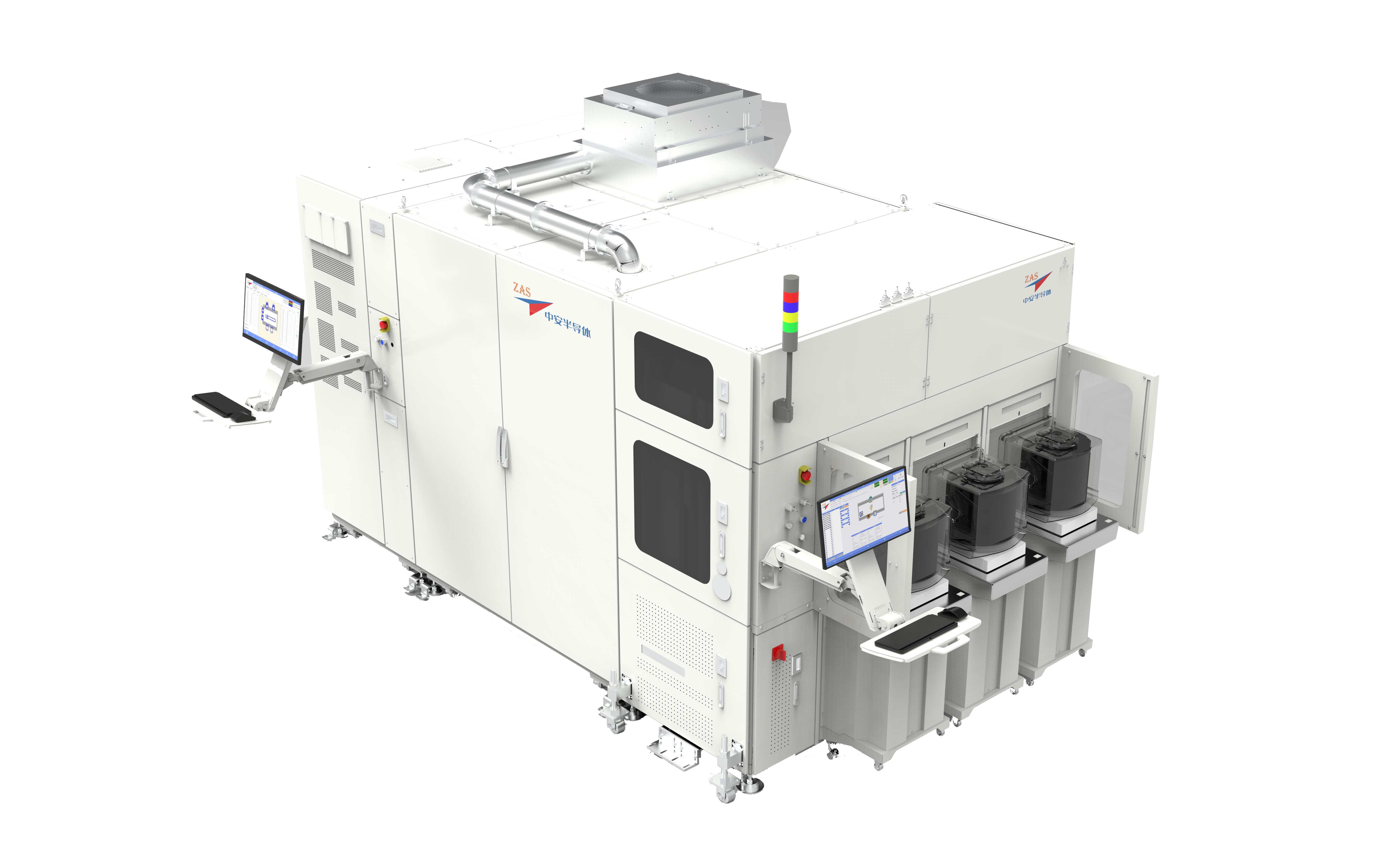
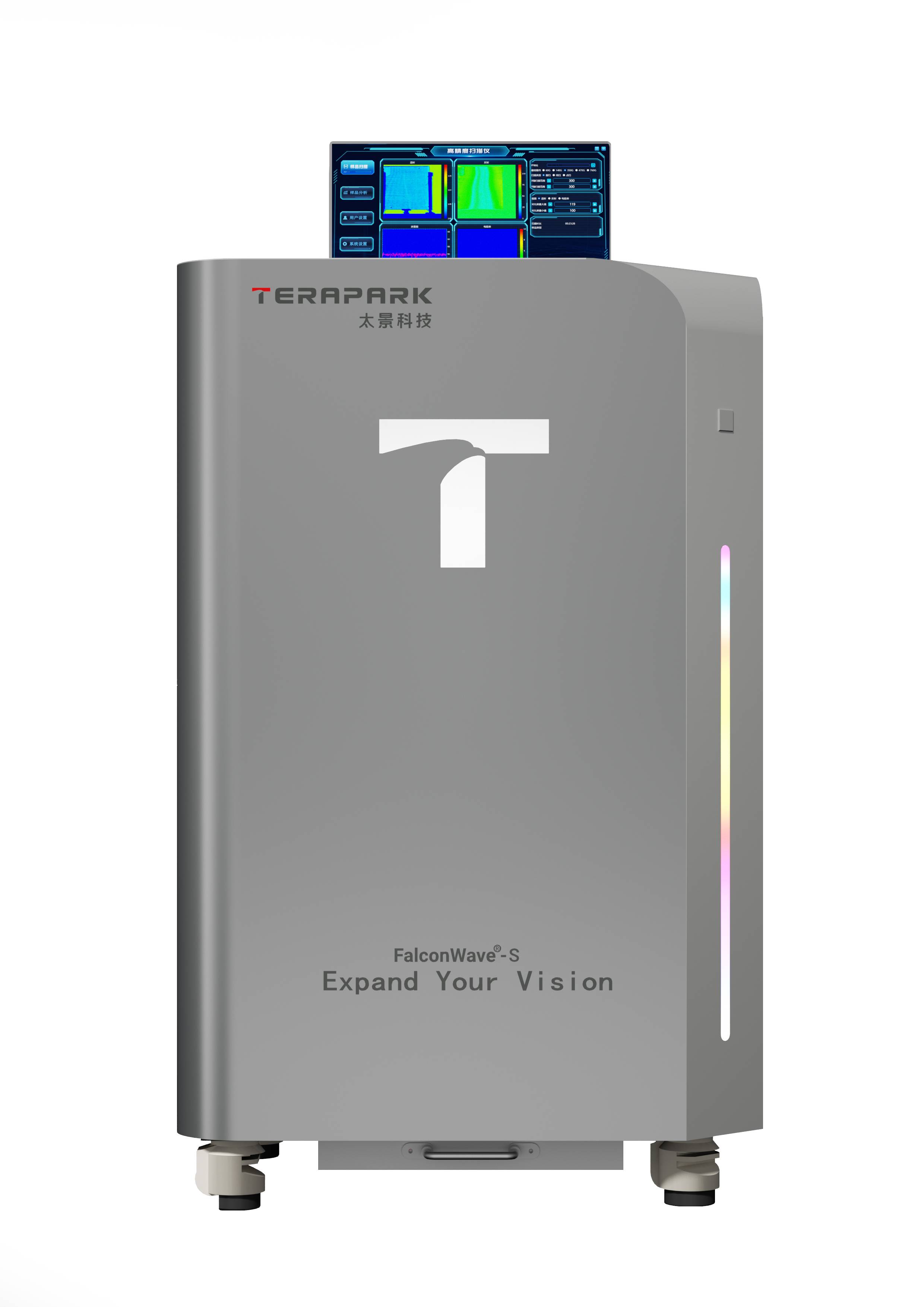
Third-Generation Semiconductor Non-Visual Particle Detection Equipment (ZPC)
Particle inspection equipment in wafer manufacturing is used to detect tiny particles or impurities on the surface or inside the wafer. These particles or impurities may adversely affect the quality and performance of the wafer, such as causing circuit shorts, failures, or reducing chip reliability. Therefore, the role of particle detection equipment is to ensure the cleanliness and quality of wafers during the manufacturing process, thereby improving the success rate of chip manufacturing and product reliability.
The ZPC equipment can quickly and accurately detect tiny particles on the surface of wafers and provide detailed analysis reports, helping manufacturers quickly identify and address potential quality issues. It measures parameters such as the size, shape, and thickness of the wafer to ensure compliance with specifications and provide reference data for subsequent processes.
Key Features and Advantages:
Comprehensive Detection: Capable of detecting all known defects on wafers, ensuring product quality and production efficiency.
Universal Applicability: Suitable for EPI and Substrate, as well as transparent and non-transparent materials, meeting the requirements of different processes and materials.
High Precision: Detects defects as small as 80nm, providing high-precision defect detection capability.
High-Speed Detection: Detection speed is significantly faster than competitors, improving production efficiency and process benefits.
DIC Technology: Utilizes DIC technology with high detection sensitivity, greatly increasing the Defect Capture Rate, enhancing detection reliability and accuracy.
Low-Noise Light Source: Equipped with a low-noise light source to ensure stability and reliability of data acquisition.
High Resolution: Utilizes a high-resolution detector, providing clear images and data for defect analysis and identification.
Advanced AI Algorithms: Equipped with advanced AI algorithms to improve data processing and analysis efficiency, accelerating the defect detection process.
Wide Wavelength Coverage: Uses 310-320nm excitation laser and detector segmentally covers fluorescence bands from 370nm to 1000nm, achieving the most comprehensive fluorescence detection.
With its comprehensive, universal, high-precision, high-speed, and advanced technological advantages, this product has become the leading choice for non-visual particle detection in the semiconductor field, providing users with reliable quality assurance and productivity enhancement.


![[Used] laser](https://cdn.sumecdtx.com/equipment/20230818/928f9346aceb42e3b60670c380399f59.jpg)