Search


 Post Requirements

 Post Requirements
Product information
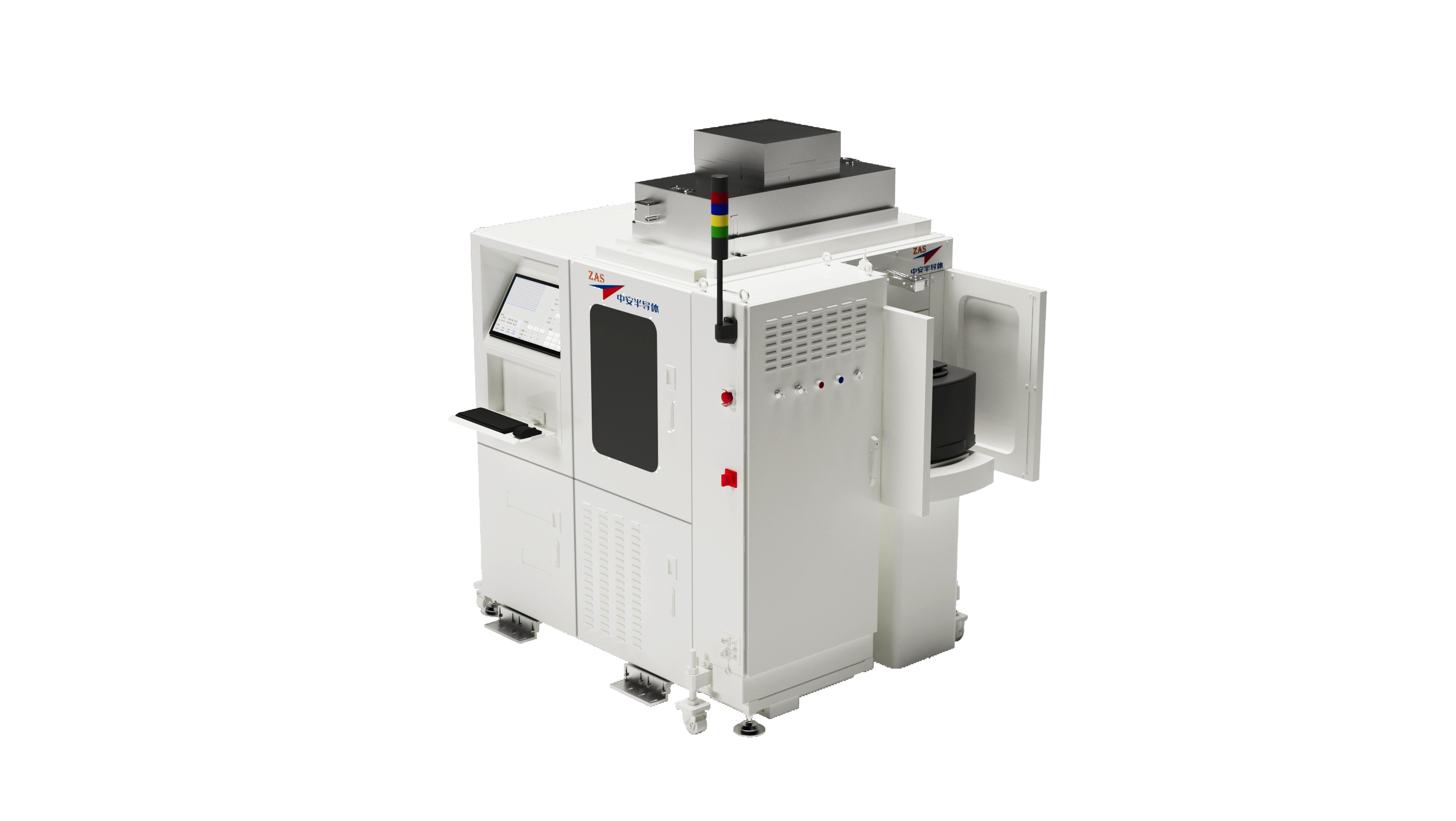
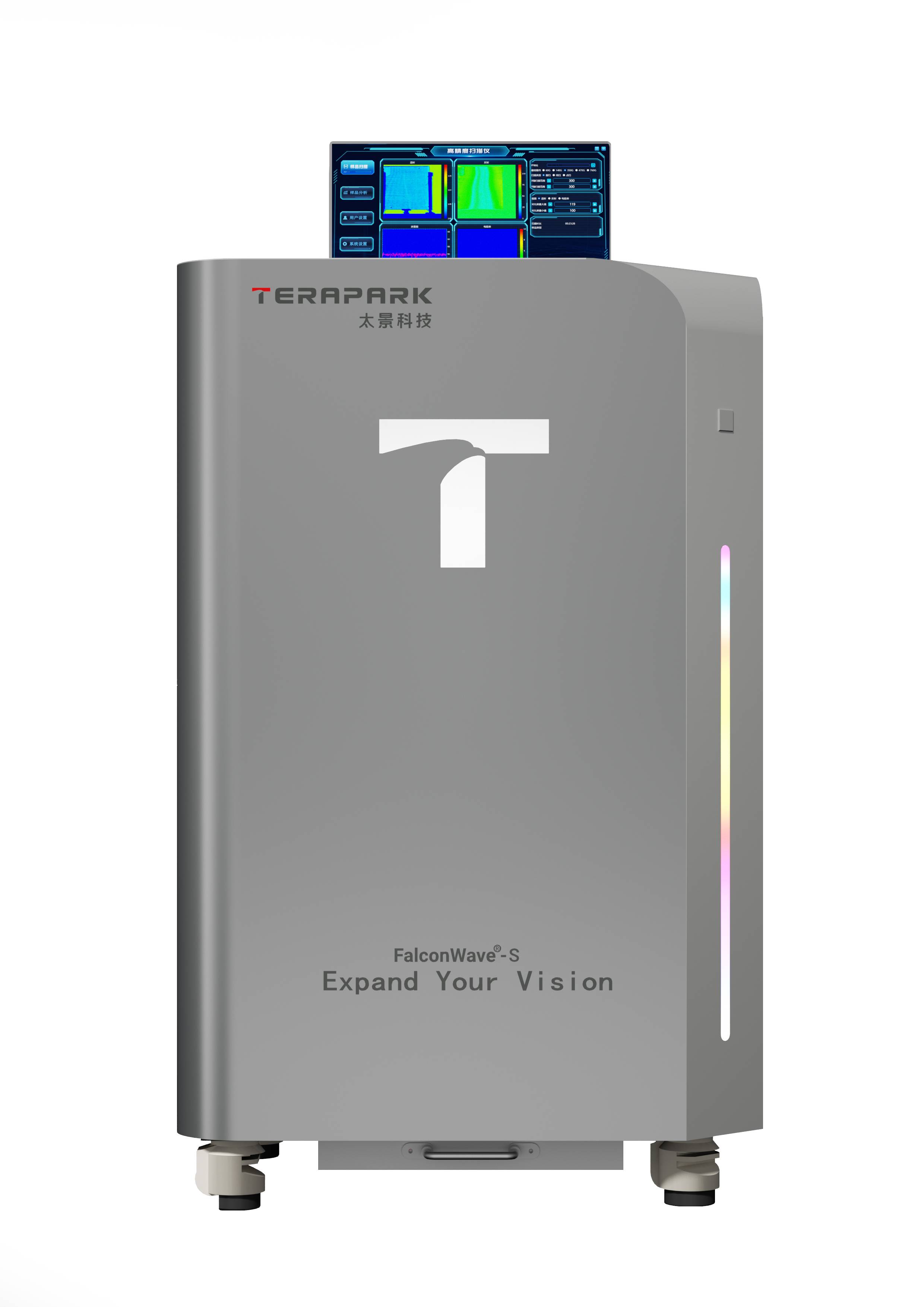
Wafer Surface Warpage and Stress Measurement Equipment (WGT-V)
Wafer geometry measurement equipment plays a crucial role in wafer manufacturing, not only in measuring the geometric parameters of wafers but also in ensuring the quality and reliability of the entire manufacturing process. Firstly, wafer manufacturing is a highly precise process, where even minor geometric deviations can lead to issues in subsequent chip manufacturing, such as circuit connectivity failure or performance degradation. Therefore, by accurately measuring parameters like diameter, thickness, and flatness of wafers, manufacturers can detect potential issues early and correct them promptly to ensure the quality and performance of the final product.
Quality control is particularly important in wafer manufacturing, as wafers serve as the foundational material for chip manufacturing, directly impacting chip performance and reliability. By using wafer geometry measurement equipment, manufacturers can effectively monitor various stages of the manufacturing process, reduce deviations and defects, lower scrap rates, and enhance production efficiency.
Key Features and Advantages:
Wide Application: Suitable for wafer manufacturing, wafer-level packaging, and semiconductor process equipment development and manufacturing fields, meeting the needs of different process production lines.
Dual-Surface Morphology and Thickness Measurement: Utilizes two spectrum confocal displacement sensors arranged in opposition to achieve high-precision measurement of both sides and thickness of wafers.
High-Precision Displacement Measurement: Spectrum confocal technology ensures high-precision displacement measurement, ensuring the accuracy and reliability of measurement results.
Accurate Measurement of Both Sides and Thickness: Opposing sensors provide precise measurements of both sides and thickness, providing comprehensive morphology and thickness information.
Multi-Line Measurement: Setting the line angle allows simultaneous measurement of multiple lines, improving measurement efficiency and data acquisition speed.
High-Density Data Points: The equipment features high-density data points, with a lateral resolution of up to 200μm, providing finer surface morphology and thickness distribution.
Advanced Algorithms: Advanced algorithms can predict the post-polishing NT map, allowing users to understand the wafer surface condition after polishing in advance, providing reference for subsequent processes.
Unaffected by Metal Contamination: The equipment is not affected by metal contamination during measurement and can accurately measure various types of wafers.
With its high precision, efficiency, and customizability, this product has become the ideal choice for wafer manufacturing and semiconductor process fields, providing users with reliable quality assurance and productivity enhancement.


![[Used] laser](https://cdn.sumecdtx.com/equipment/20230818/928f9346aceb42e3b60670c380399f59.jpg)