

 Search


 Post Requirements

 Post Requirements
Product information
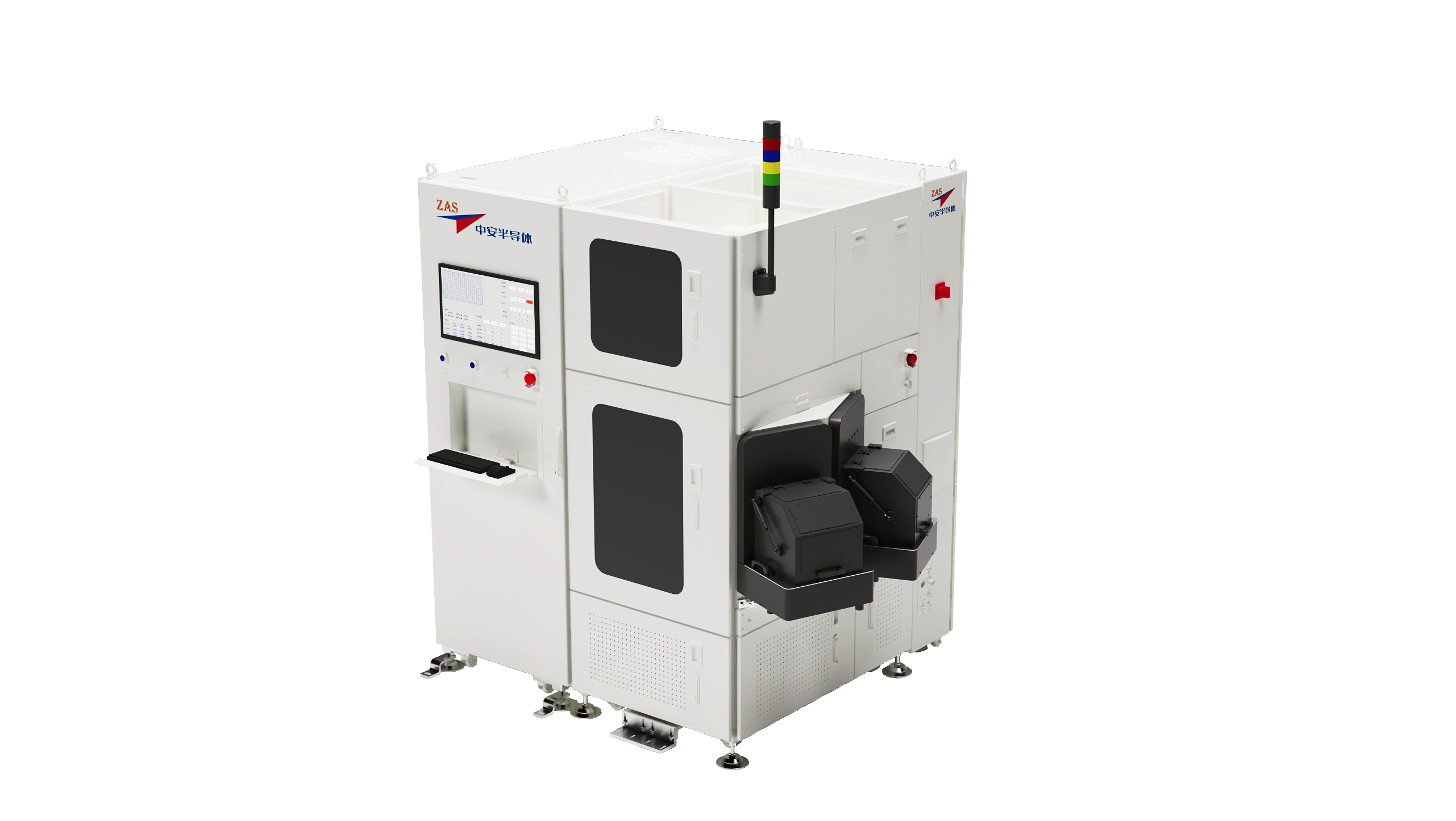
6/8'' Wafer Surface Warpage and Nanotopography Measurement Equipment (WGT-V)
Wafer geometry measurement equipment plays a crucial role in wafer manufacturing, not only in measuring the geometric parameters of wafers but also in ensuring the quality and reliability of the entire manufacturing process. Firstly, wafer manufacturing is a highly precise process, where even minor geometric deviations can lead to issues in subsequent chip manufacturing, such as circuit connectivity failure or performance degradation. Therefore, by accurately measuring parameters like diameter, thickness, and flatness of wafers, manufacturers can detect potential issues early and correct them promptly to ensure the quality and performance of the final product.Quality control is particularly important in wafer manufacturing, as wafers serve as the foundational material for chip manufacturing, directly impacting chip performance and reliability. By using wafer geometry measurement equipment, manufacturers can effectively monitor various stages of the manufacturing process, reduce deviations and defects, lower scrap rates, and enhance production efficiency.
Key Features and Advantages:
Wide Application: Suitable for wafer manufacturing, wafer-level packaging, and semiconductor process equipment development and manufacturing fields, meeting the needs of different industries;
Optical Interference Detection: Utilizes optical interference detection technology to achieve high-precision measurement of wafer surface warpage and flatness through the analysis of multiple surface interference fringes;
Patented Air Bearing Chuck: Equipped with a patented air bearing chuck, ensuring true contact-free measurement process, thereby avoiding human interference and wafer damage;
Single Image Acquisition: Supports single image acquisition to obtain data on wafer shape, flatness, roughness, etc., enhancing measurement efficiency and data acquisition speed;
Comprehensive and Intuitive Data Presentation: Provides comprehensive and intuitive data presentation, offering users clear and visual measurement results for analysis and decision-making;
After-Sales Service and Warranty Policy: We provide comprehensive after-sales service and warranty policy to ensure smooth and worry-free usage for customers;
The high precision, efficiency, and user-friendliness of this product make it an ideal choice for wafer manufacturing and semiconductor process fields, providing users with reliable quality assurance and productivity enhancement.


![[Second-hand] laser](https://cdn.sumecdtx.com/equipment/20230818/928f9346aceb42e3b60670c380399f59.jpg)


