

 Search


1 / 1
Laser Induced Crystallization


Price:
price negotiable
Brand Name:
LasTop TechnologyCountry Region:
ChinaModel No:
LIC
 Post Requirements
LasTop Technology 
Country: China
Main Products: Wafer laser annealing, wafer laser marking, wafer laser debonding, wafer laser slotting, wafer laser slicing, wafer level laser marking, fully automatic laser glue removal, IC fully automatic laser marking, frame laser marking, and three light spot inspection
View more
Price:
price negotiable
Brand Name:
LasTop TechnologyCountry Region:
ChinaModel No:
LIC
 Post Requirements
LasTop Technology 
China
Main Products:
Wafer laser annealing, wafer laser marking, wafer laser debonding, wafer laser slotting, wafer laser slicing, wafer level laser marking, fully automatic laser glue removal, IC fully automatic laser marking, frame laser marking, and three light spot inspection
Product information
Laser Induced Crystallization | LIC
Application
Laser crystallization of
amorphous materials and
in-situ dopant activation
Product Features
The world's first, 12 inch mass production facility
Independly developped optical system with LIET technology enables high uniformity
Energy density accuracy down to 5mJ/cm2
nS level pulse width control
| Technical specification | |
| Laser wavelength | 527nm |
| Wafer size | 12 inch |
| Energy modulation accuracy | 5mJ/cm2 |
| uniformity of beam top | ≤1% |
| Focal depth range | 5mm |
All products in the store
Strip Laser Marking
IC framework Laser Marking
Laser Debonding
Wafer Laser Marking
Laser Decapping
Fiber Laser High Speed Marking

You May Like


冷热台
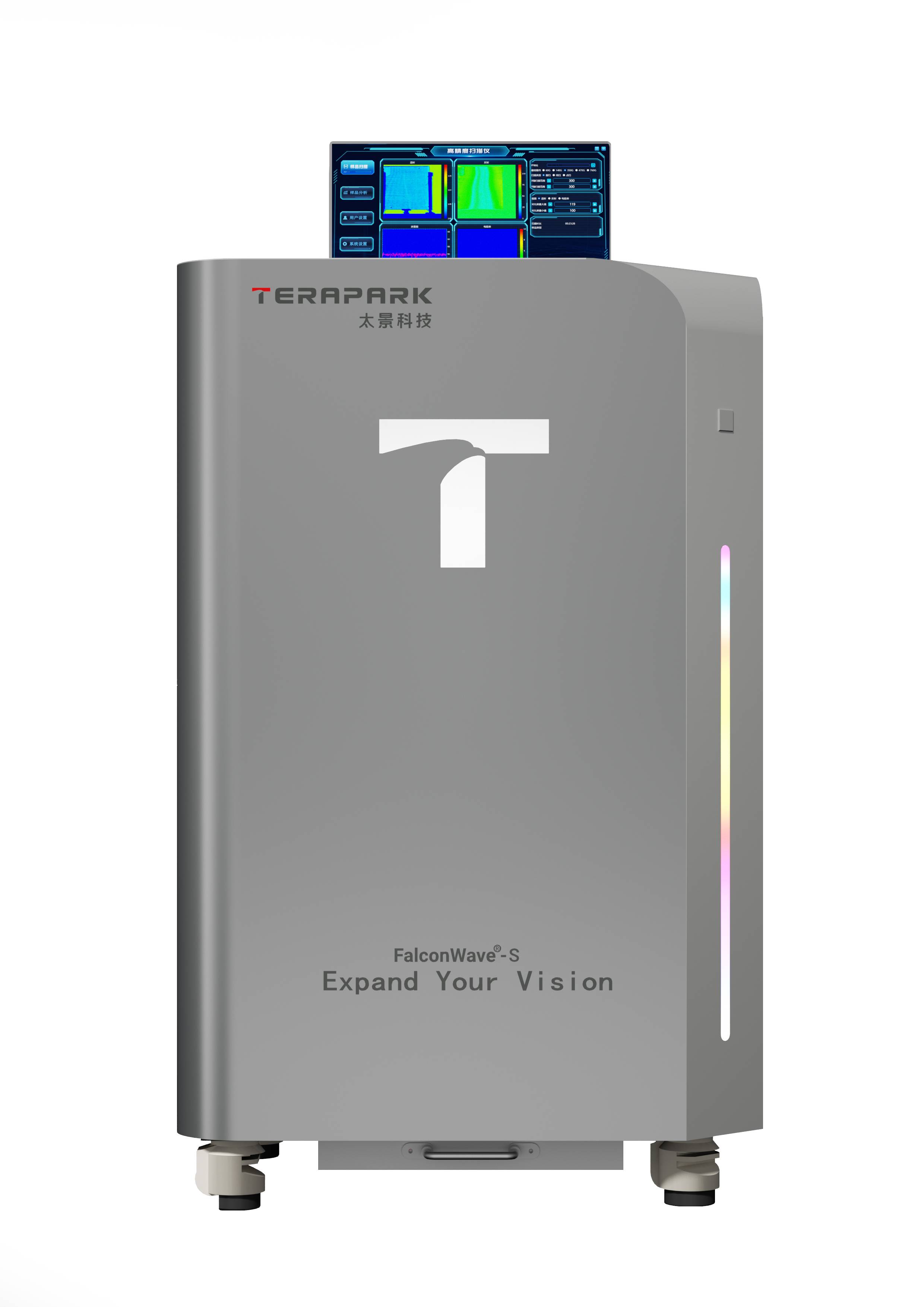
FalconWave®-S High Resolution Product
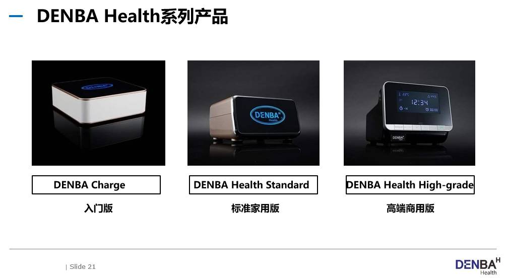
DENBA HEALTH

Thin film laser flash thermal conductivity meter+laser thermal conductivity meter

Test platform for electro-optical parameters of focal plane detector
![[Second-hand] laser](https://cdn.sumecdtx.com/equipment/20230818/928f9346aceb42e3b60670c380399f59.jpg)
[Second-hand] laser

德国Mahr原装进口轮廓仪MarSurf XC 2轮廓仪

Adcole OptiShaft Measuring Machine

LuphoScan 50SL高速非接触式3D非球面光学面形测量系统

HyTron