

 Search


1 / 1
LasTop Technology IGBT Laser Annealing


Price:
price negotiable
Brand Name:
LasTop TechnologyCountry Region:
ChinaModel No:
LA
 Post Requirements
LasTop Technology 
Country: China
Main Products: Wafer laser annealing, wafer laser marking, wafer laser debonding, wafer laser slotting, wafer laser slicing, wafer level laser marking, fully automatic laser glue removal, IC fully automatic laser marking, frame laser marking, and three light spot inspection
View more
Price:
price negotiable
Brand Name:
LasTop TechnologyCountry Region:
ChinaModel No:
LA
 Post Requirements
LasTop Technology 
China
Main Products:
Wafer laser annealing, wafer laser marking, wafer laser debonding, wafer laser slotting, wafer laser slicing, wafer level laser marking, fully automatic laser glue removal, IC fully automatic laser marking, frame laser marking, and three light spot inspection
Product information
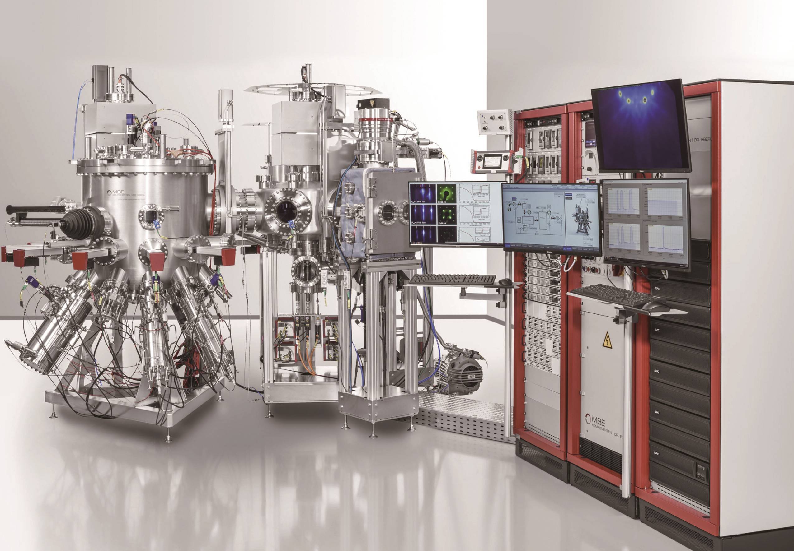
IGBT Laser Annealing | LA
Application
Ion-activation for silicon IGBT
Product Features
High reliability and stability
Independly developped Optical system
Excellent thermal budget control
50μm ultra-thin TaiKo wafer handling capability
| Technical specification | ||||
| Wafer size | 6 inch, 8 inch, 12 inch | |||
| Laser power | 60W*2 | 90W*2 | 60W*2+300W | 90W*2+300W |
| Laser energy density | ≥5J/cm2×2 | |||
| Activation efficiency | ≥95%@B+ | ≥90%@P+ | ||
| RS non-uniformity | WIW:≤1%@3sigma | WTW:≤1%@3sigma | ||
All products in the store
Strip Laser Marking
IC framework Laser Marking
Laser Debonding
Wafer Laser Marking
Laser Decapping
Fiber Laser High Speed Marking

You May Like

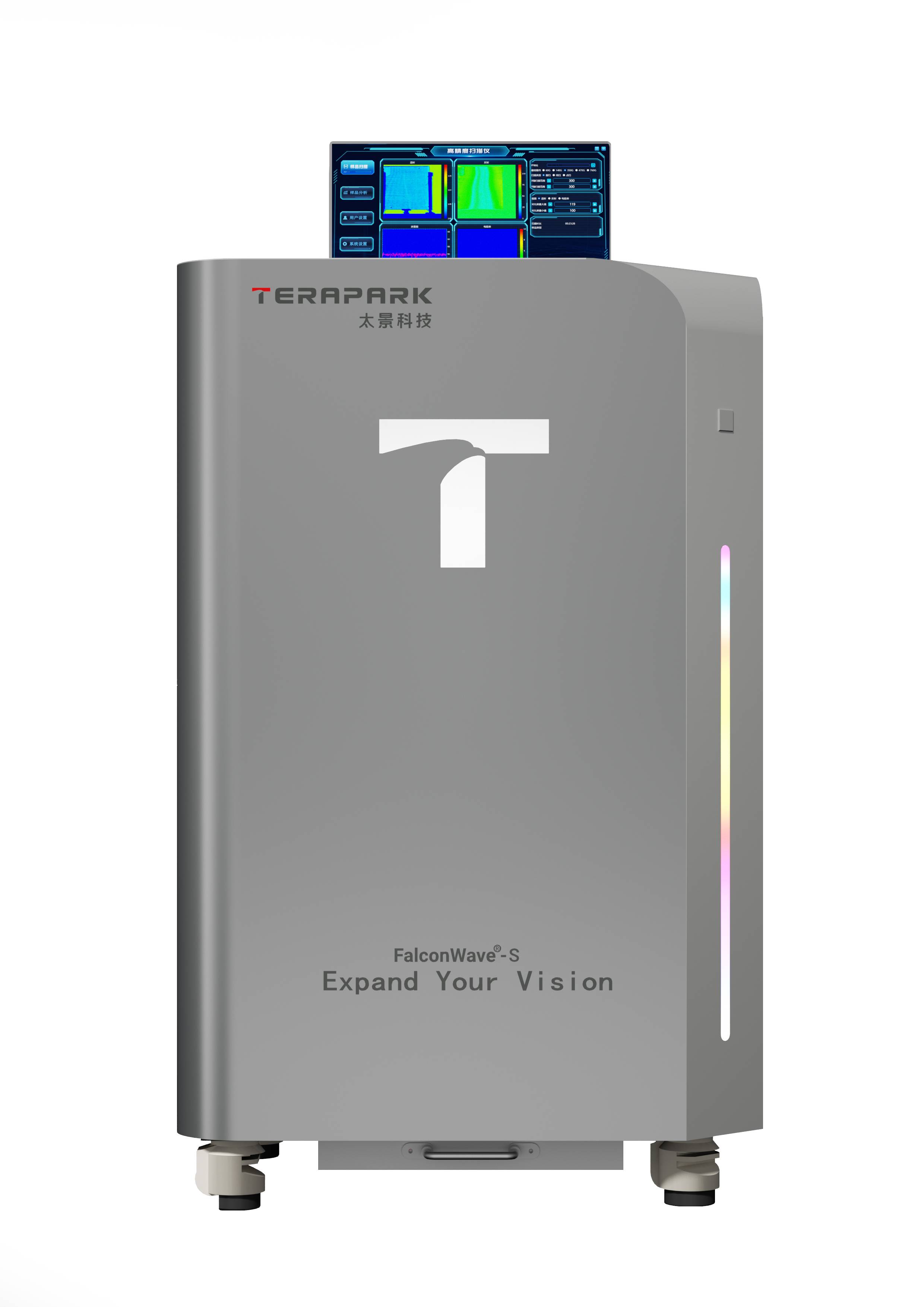
FalconWave®-S High Resolution Product
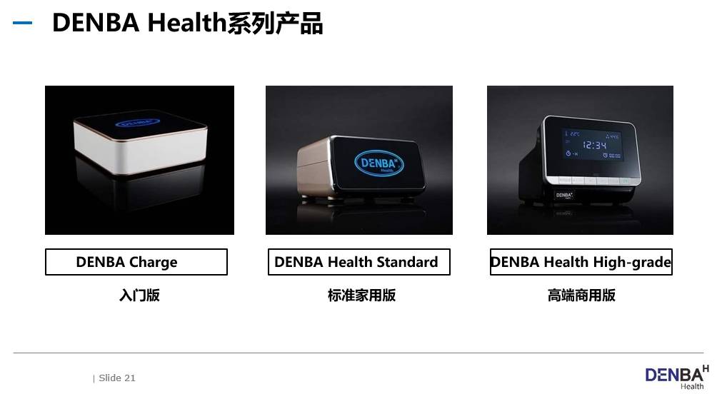
DENBA HEALTH
![[Used] laser](https://cdn.sumecdtx.com/equipment/20230818/928f9346aceb42e3b60670c380399f59.jpg)
[Used] laser
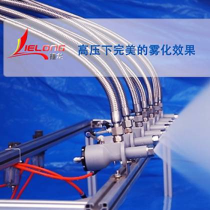
High pressure atomization and spraying system
6/8 inch resistor long crystal furnace
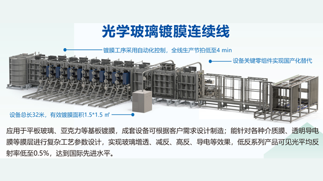
Optical anti-reflection coating continuous line
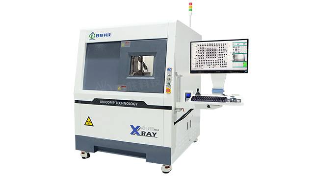
Electronic manufacturing of X-Ray inspection equipment
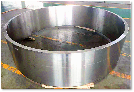
Titanium products、Copper alloy products
IR Vertical Impregnation Machine
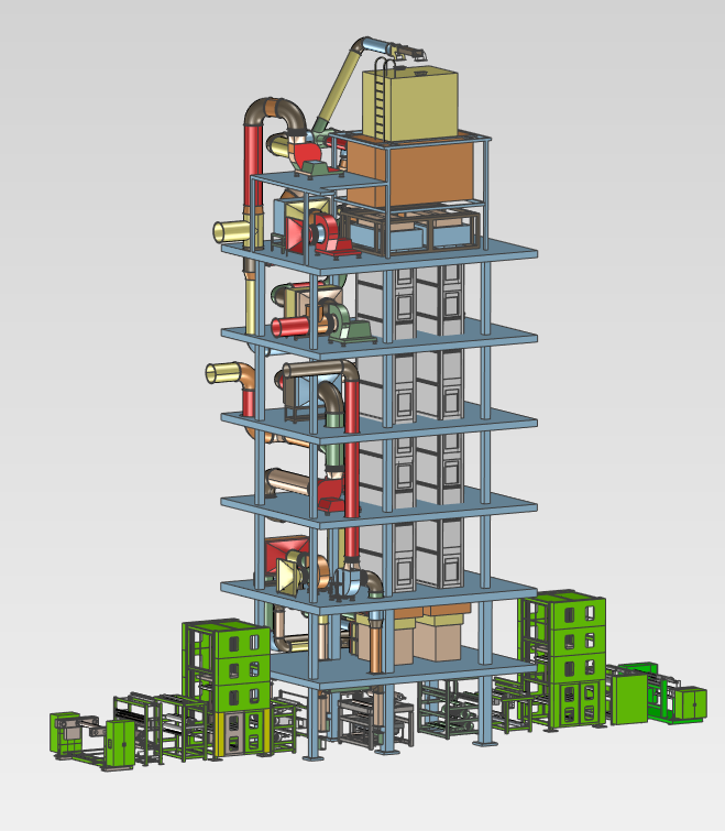
Molecular beam epitaxial system MBE