

 Search


1 / 1
AK Optics SiC Wafer Defect Inspection System


Price:
price negotiable
Brand Name:
AK Optics Country Region:
ChinaModel No:
E3500
 Post Requirements
AK Optics 
Country: China
Main Products:
View more
Price:
price negotiable
Brand Name:
AK Optics Country Region:
ChinaModel No:
E3500
 Post Requirements
AK Optics 
China
Main Products:
Product information
The E3500 is a defect inspection equipment specifically designed for SiC wafers. It can inspect surface and fluorescent defects in SiC substrates and epitaxial wafers. This equipment can identify and differentiate between defects such as triangle, carrot, downfall, micropipe, SF (stacking fault), and BPD (basal plane dislocation). It supports inspection of 4", 6", and 8" wafers, offering high throughput and high inspection accuracy.
Wafer Size
Size: 4", 6", 8" compatible;
2 cassettes; other sizes upon requests
Thickness:350um~1500um(Other thicknesses need to be tested)
Defect Inspection Capability
SiC Substrate:Particle、Scratch、pit、bump、stain、Micro Pipe、KOH Etch Mapping、SF
SiC Epi:Particle、Scratch、pit、bump、Carrot&Surface Triangle、Downfall、KOH Etch Mapping、SF,BPD
*It can identify pits and bumps as small as 0.18µm.
All products in the store
F2000 Particle counter
H2000 integrated circuit graphic wafer front defects
Wafer Surface Profile Inspection and Sorting System
SiC Wafer Defect Inspection System

You May Like

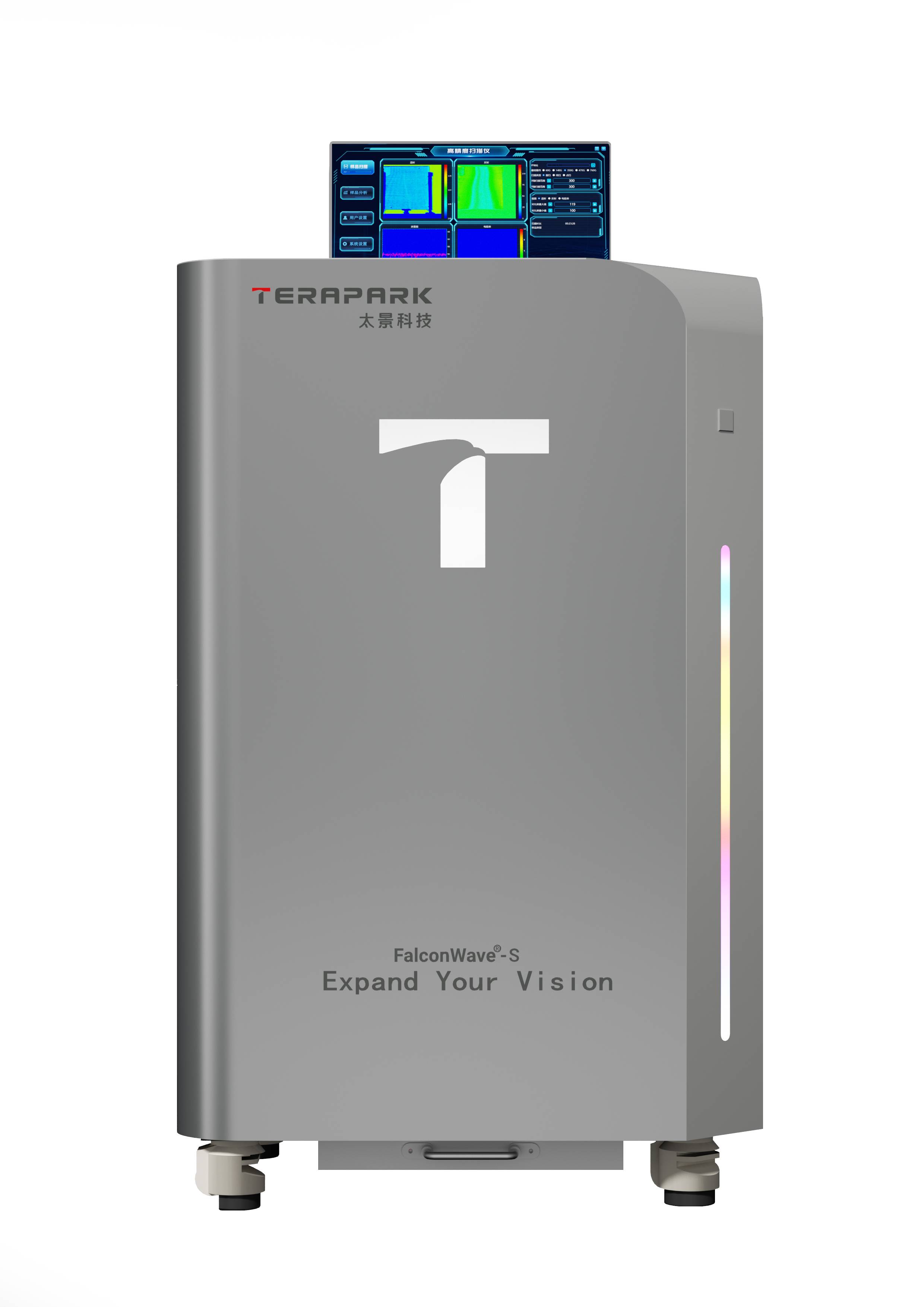
FalconWave®-S High Resolution Product
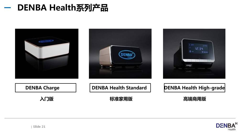
DENBA HEALTH
![[Used] laser](https://cdn.sumecdtx.com/equipment/20230818/928f9346aceb42e3b60670c380399f59.jpg)
[Used] laser
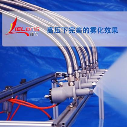
High pressure atomization and spraying system
6/8 inch resistor long crystal furnace
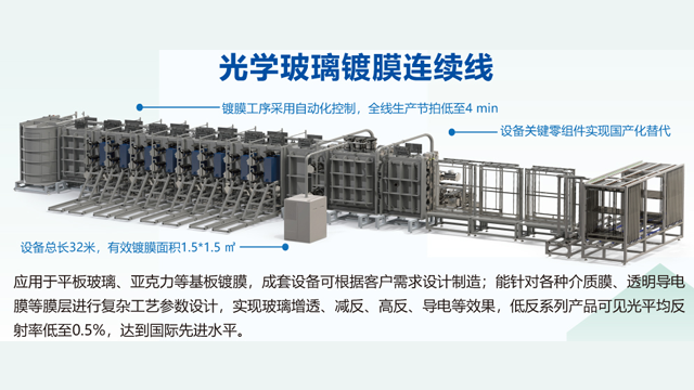
Optical anti-reflection coating continuous line
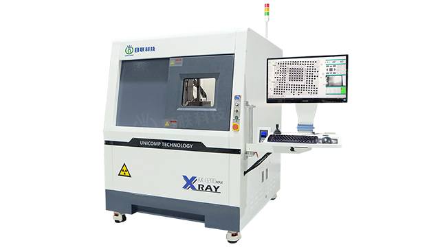
Electronic manufacturing of X-Ray inspection equipment
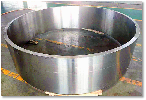
Titanium products、Copper alloy products
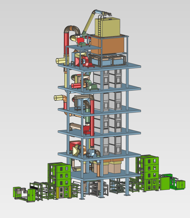
IR Vertical Impregnation Machine
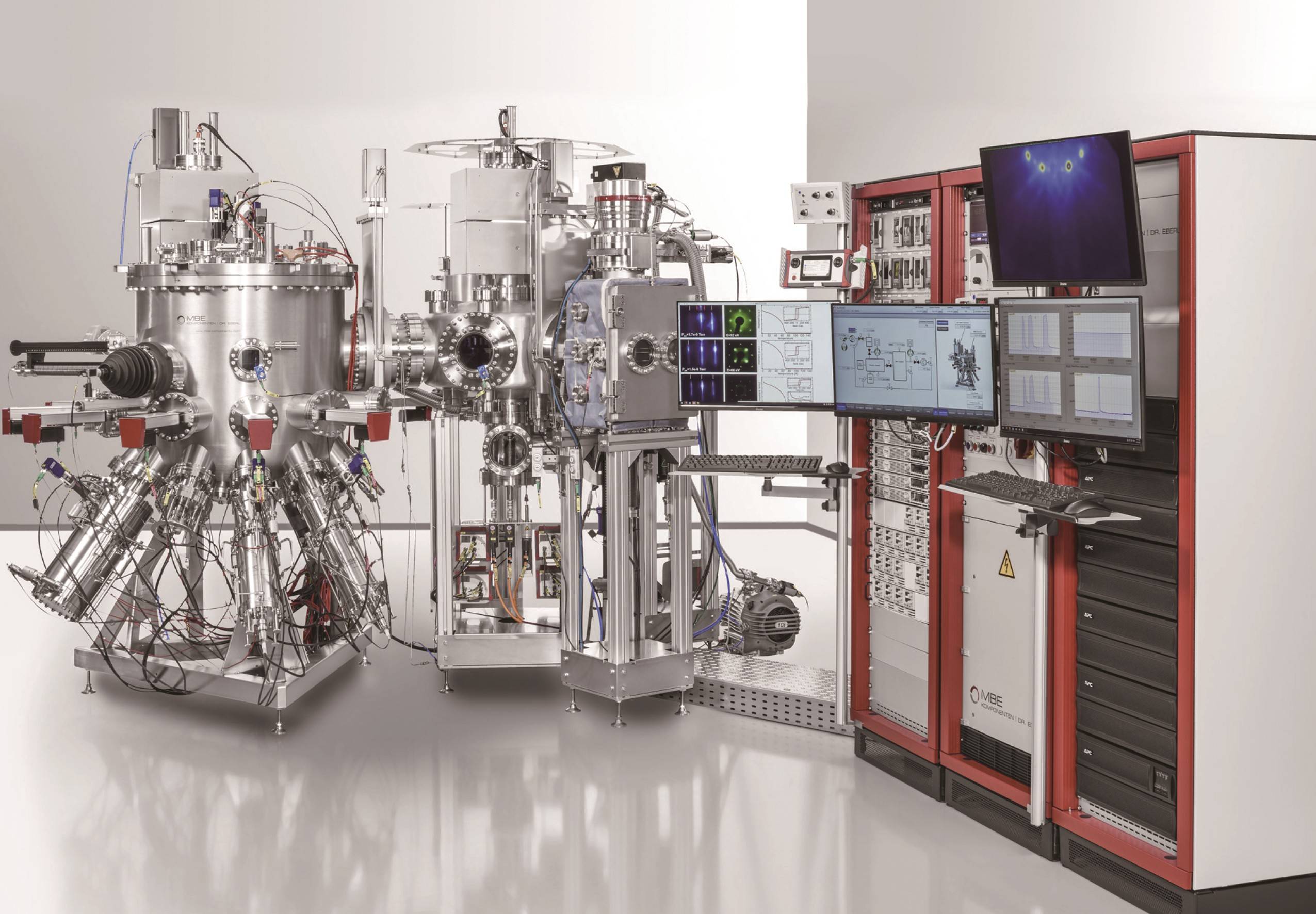
Molecular beam epitaxial system MBE