

 Search


1 / 1
AK Optics Wafer Surface Profile Inspection and Sorting System


Price:
price negotiable
Brand Name:
AK Optics Country Region:
ChinaModel No:
SPI300
 Post Requirements
AK Optics 
Country: China
Main Products:
View more
Price:
price negotiable
Brand Name:
AK Optics Country Region:
ChinaModel No:
SPI300
 Post Requirements
AK Optics 
China
Main Products:
Product information
The SPI300 geometry measurement equipment
Wafer Size Compatibility**: 4", 6", 8" compatible
Standard configuration includes 16 cassettes or 14 cassettes (optional/WA), with all cassettes freely configurable for loading and unloading, allowing for flexible sorting.
Inspections category: Thickness, TTV, bow, warp, TIR (Total Indicated Reading), sori, sag, LTV (requires full map inspection).
SPI300 can output CSV data reports and allows for customized saving of line scan and area scan 2D/3D surface profile PDF reports.
Measurement Specifications
Wafer Thickness Range: 400µm - 2000µm
Probe Resolution: 0.028µm
Measurement Accuracy: ±0.2µm
Repeatability: 3σ ≤ 1.0µm
Accuracy: THK/Bow/Warp linearity ≥ 95% , TTV/TIR linearity ≥ 90%
Software Features
Function Blocks: Wafer handling control, status indication, safety interlock, data acquisition, wafer sorting, measurement result data viewing and storage, recipe editing and management, equipment status logging.
User Permissions: Engineer, Operator
Grading Function: The grading function allows user to define product grades A/B/C/NG based on their requirements.
Parameter Definition: User can independently set inspection parameters and control standards.
All products in the store
F2000 Particle counter
H2000 integrated circuit graphic wafer front defects
Wafer Surface Profile Inspection and Sorting System
SiC Wafer Defect Inspection System

You May Like

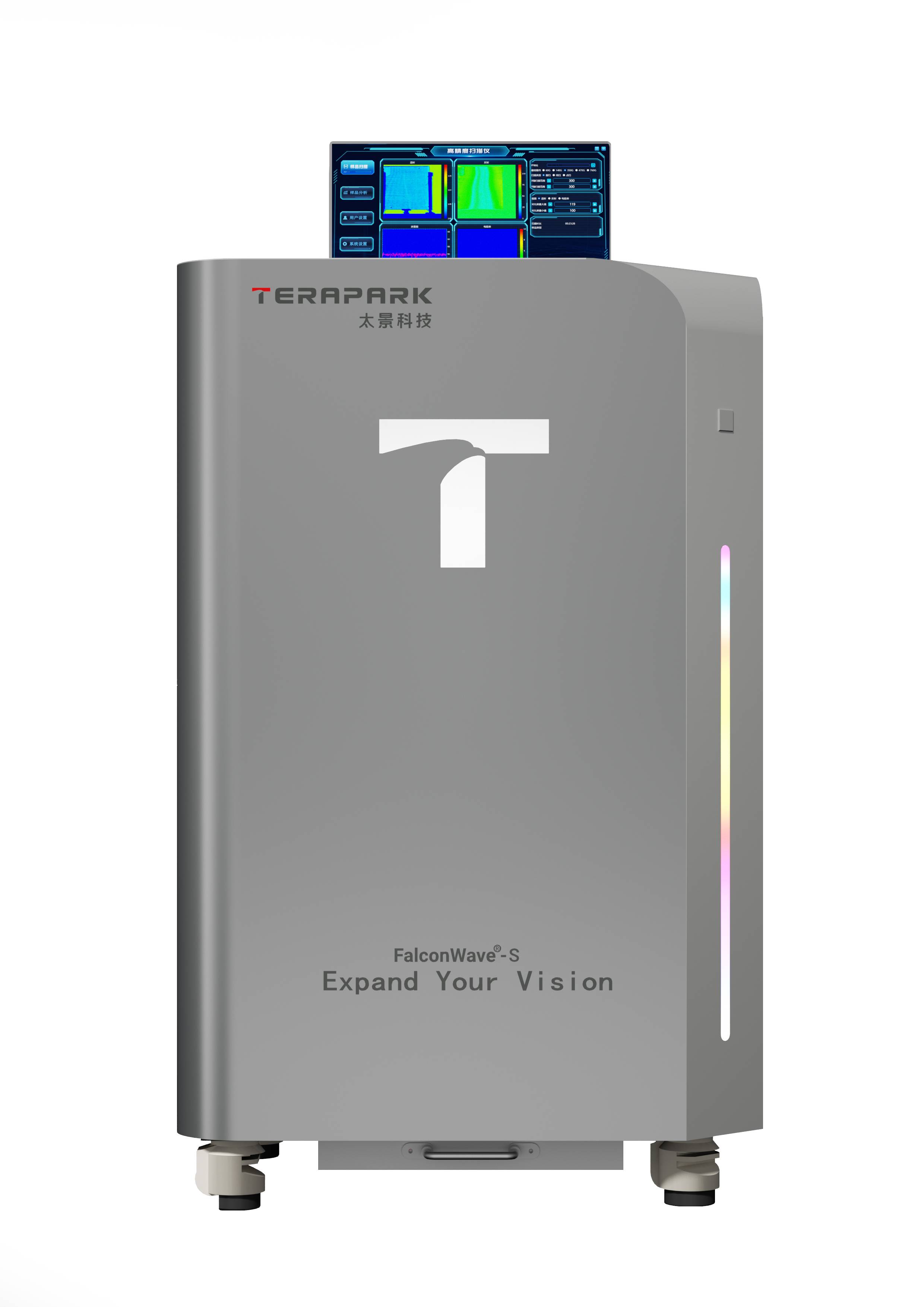
FalconWave®-S High Resolution Product
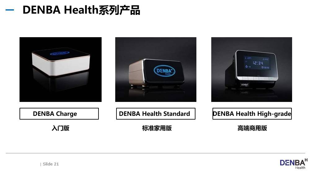
DENBA HEALTH
![[Used] laser](https://cdn.sumecdtx.com/equipment/20230818/928f9346aceb42e3b60670c380399f59.jpg)
[Used] laser
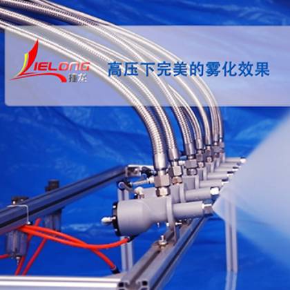
High pressure atomization and spraying system
6/8 inch resistor long crystal furnace
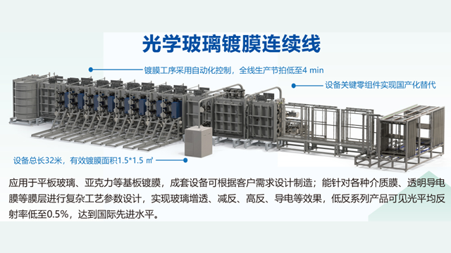
Optical anti-reflection coating continuous line
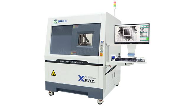
Electronic manufacturing of X-Ray inspection equipment
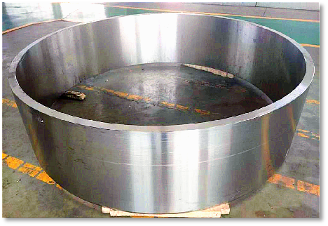
Titanium products、Copper alloy products
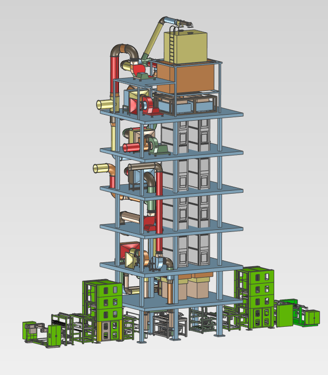
IR Vertical Impregnation Machine
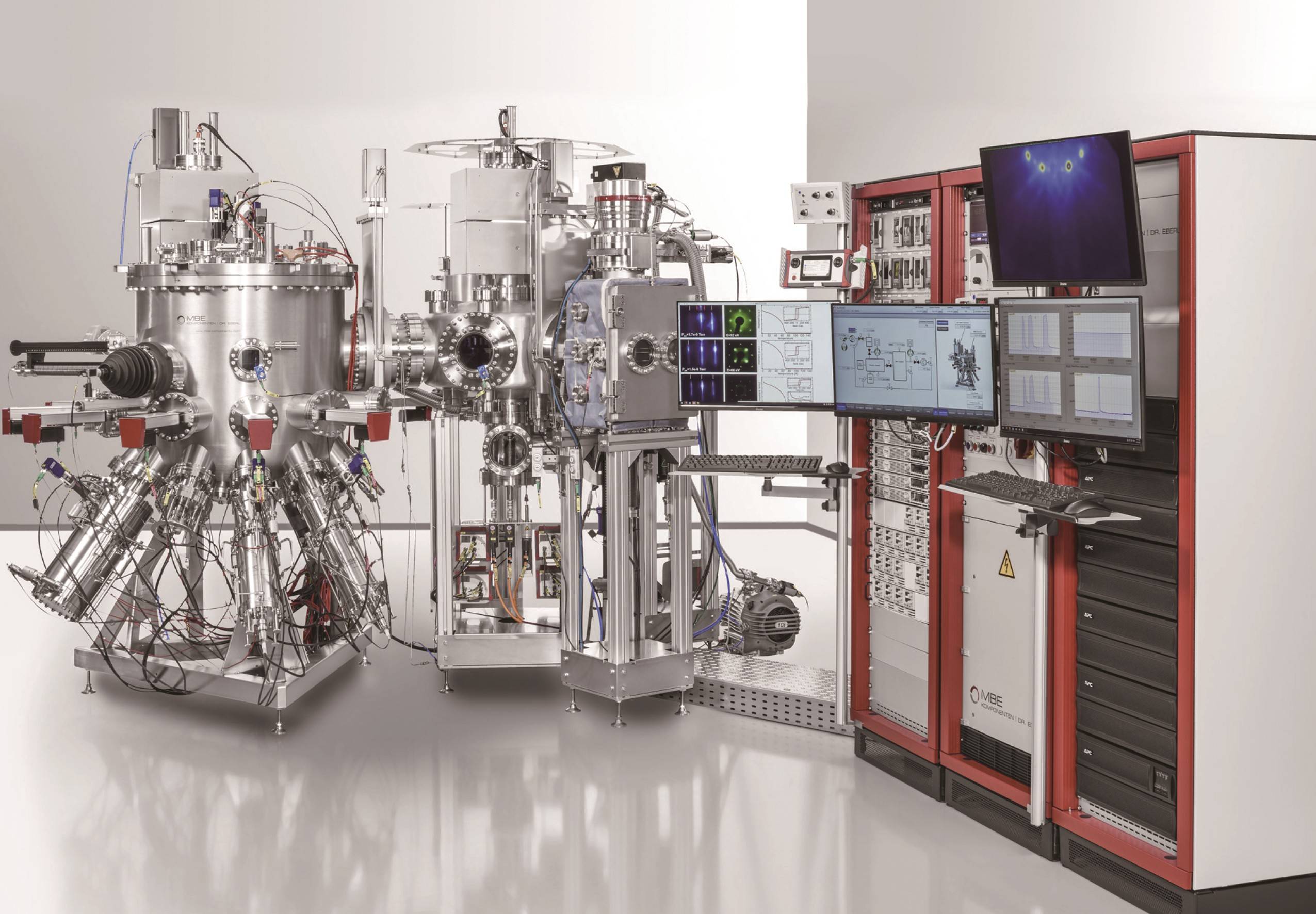
Molecular beam epitaxial system MBE