

 Search


1 / 1
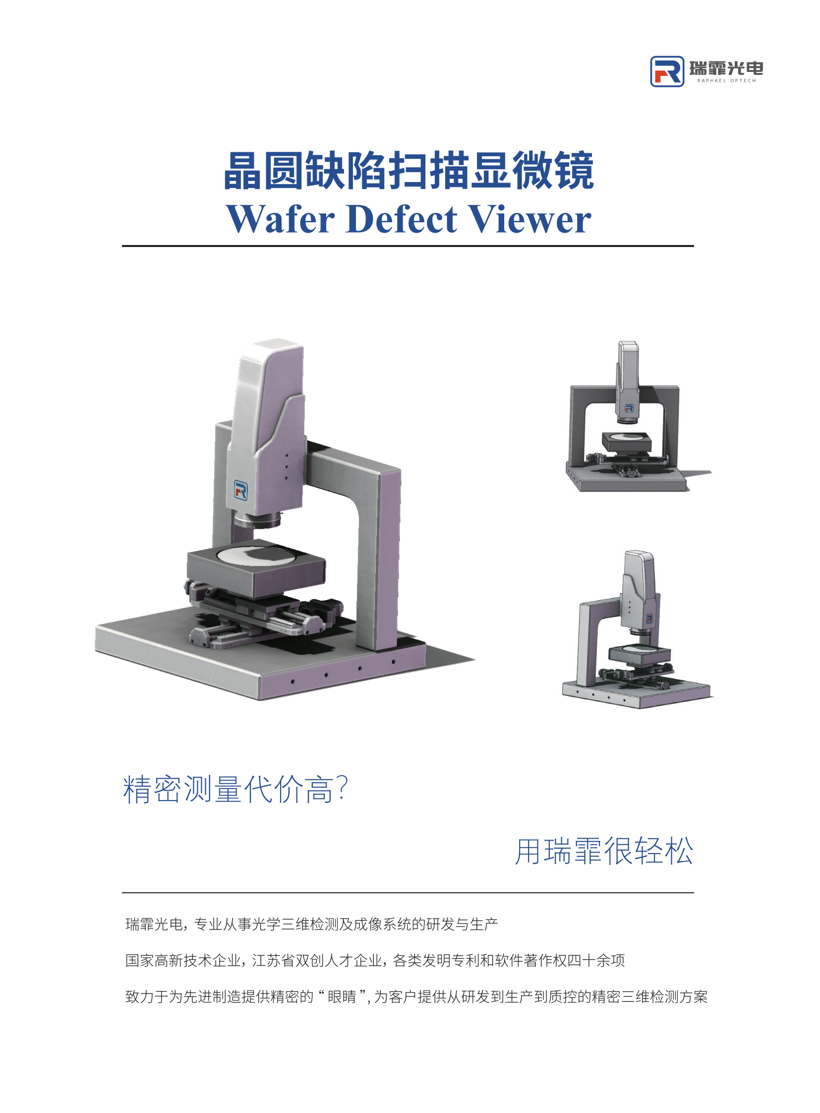
RAPHAEL OPTECH Wafer Defect Viewer


Price:
price negotiable
Brand Name:
RAPHAEL OPTECHCountry Region:
ChinaModel No:
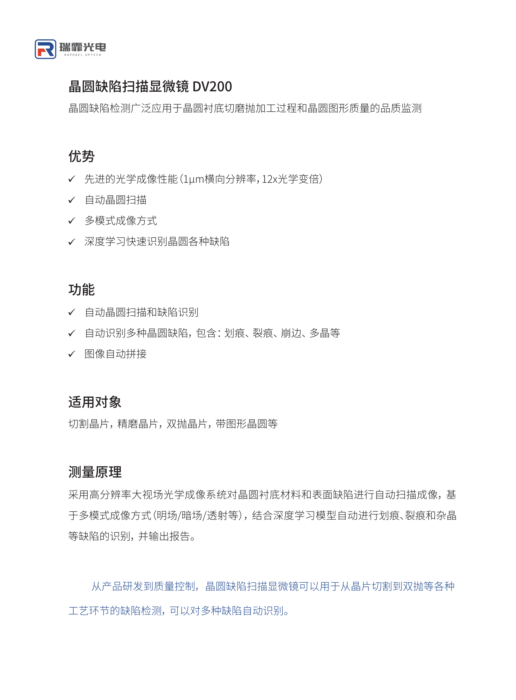
DV200
 Post Requirements
RAPHAEL OPTECH 
Country: China
Main Products: Free-form surface measurement instrument, wafer warped film stress measurement instrument, three-dimensional measurement microscope, internal stress detection instrument, super depth of field microscope, etc
View more
Price:
price negotiable
Brand Name:
RAPHAEL OPTECHCountry Region:
ChinaModel No:
DV200
 Post Requirements
RAPHAEL OPTECH 
China
Main Products:
Free-form surface measurement instrument, wafer warped film stress measurement instrument, three-dimensional measurement microscope, internal stress detection instrument, super depth of field microscope, etc
Product information
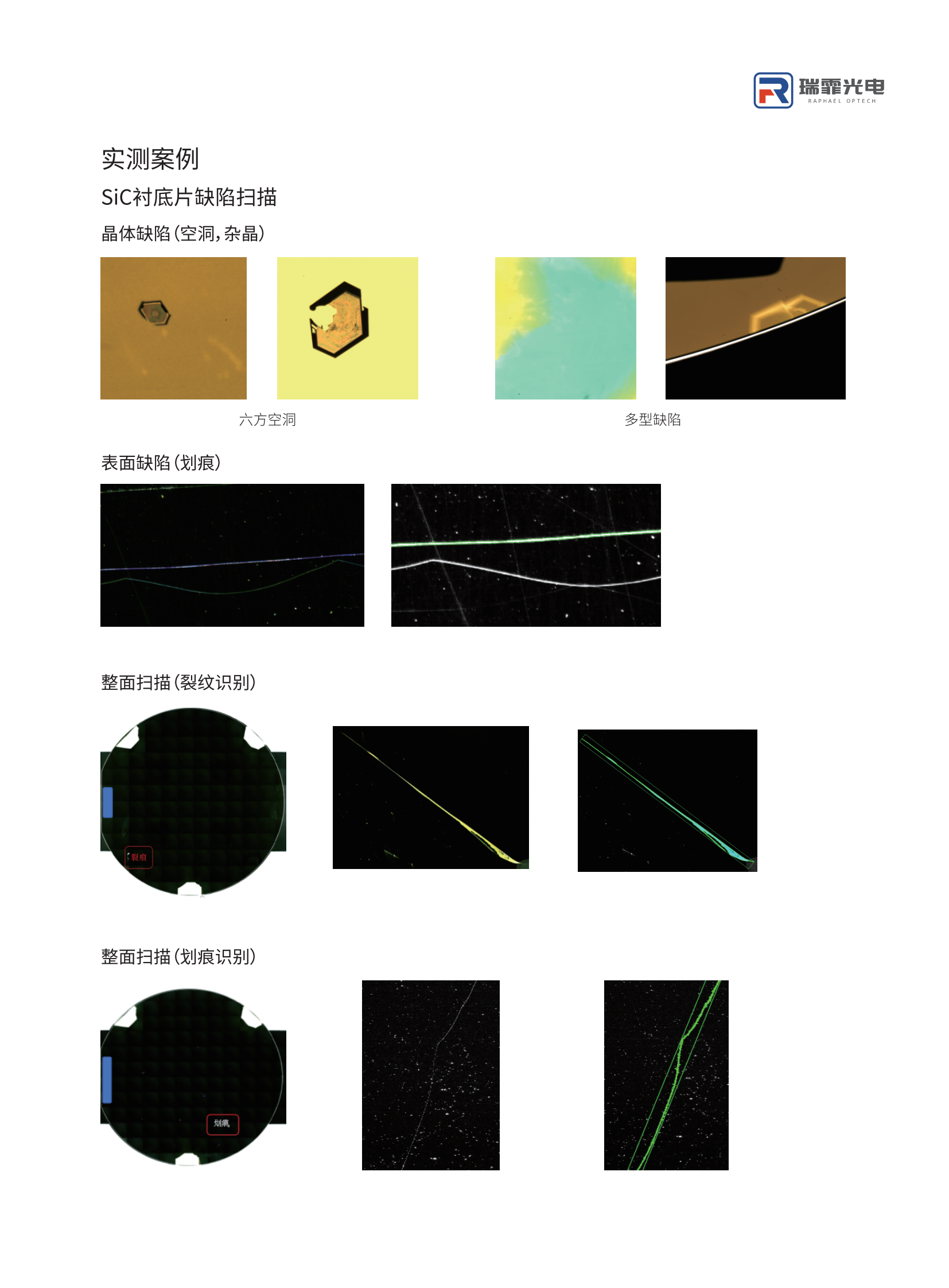
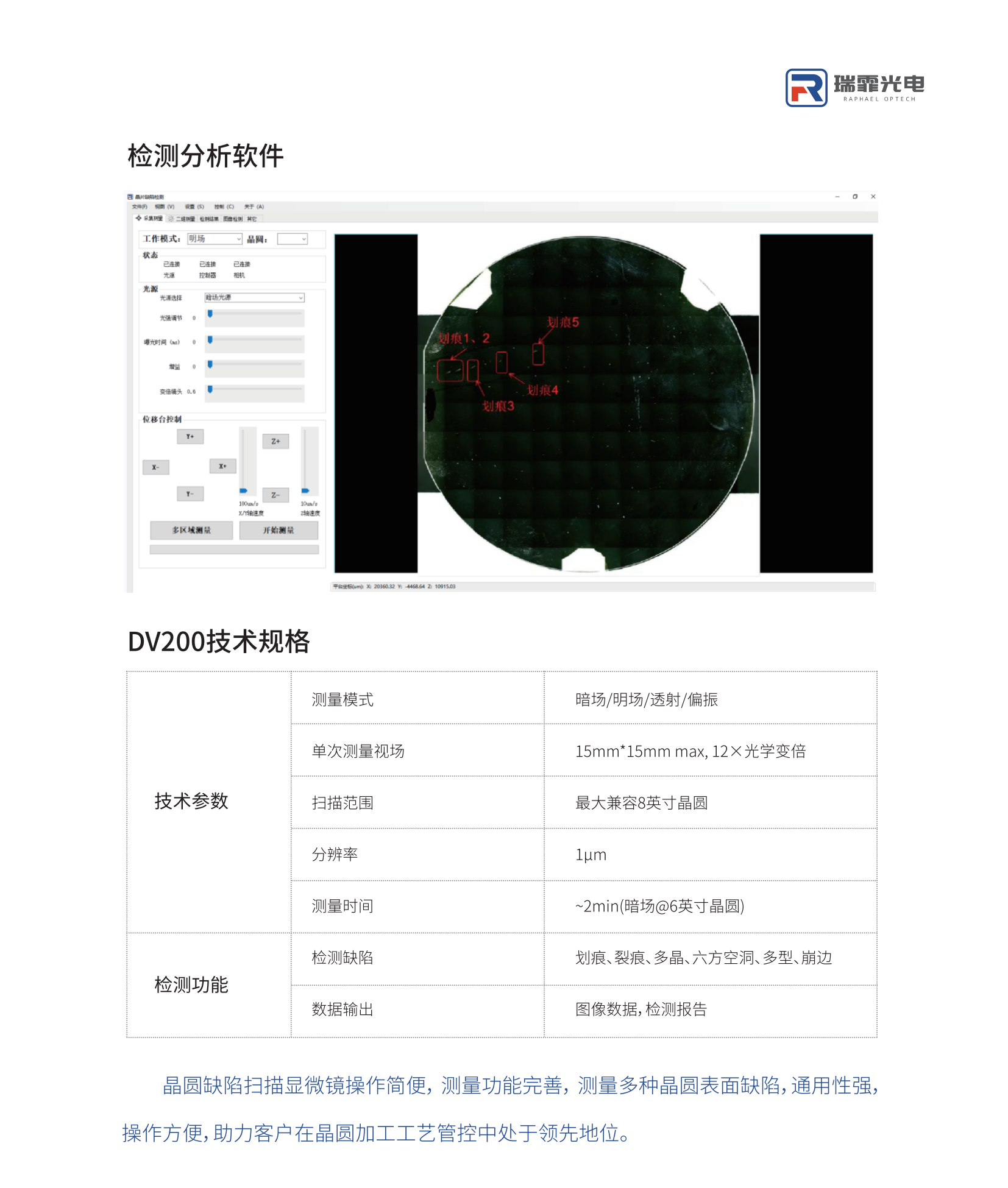
Advantages Advanced optical imaging performance (1um lateral resolution, 12x optical zoom) Automatic wafer scanning Multi-modal imaging method Deep learning Rapid identification of various wafer defects Function Automatic wafer scanning and defect identification Automatic identification of various wafer defects, including: Automatic stitching of scratches, cracks, edges, polycrystalline and other images
All products in the store
Multi-mod 3D measuring microscope
Strain Viewer
White light interference for 3D measuring microscope
Stress Mapper
FF series Freeform Optics 3D Profiler
Strain Viewer

You May Like

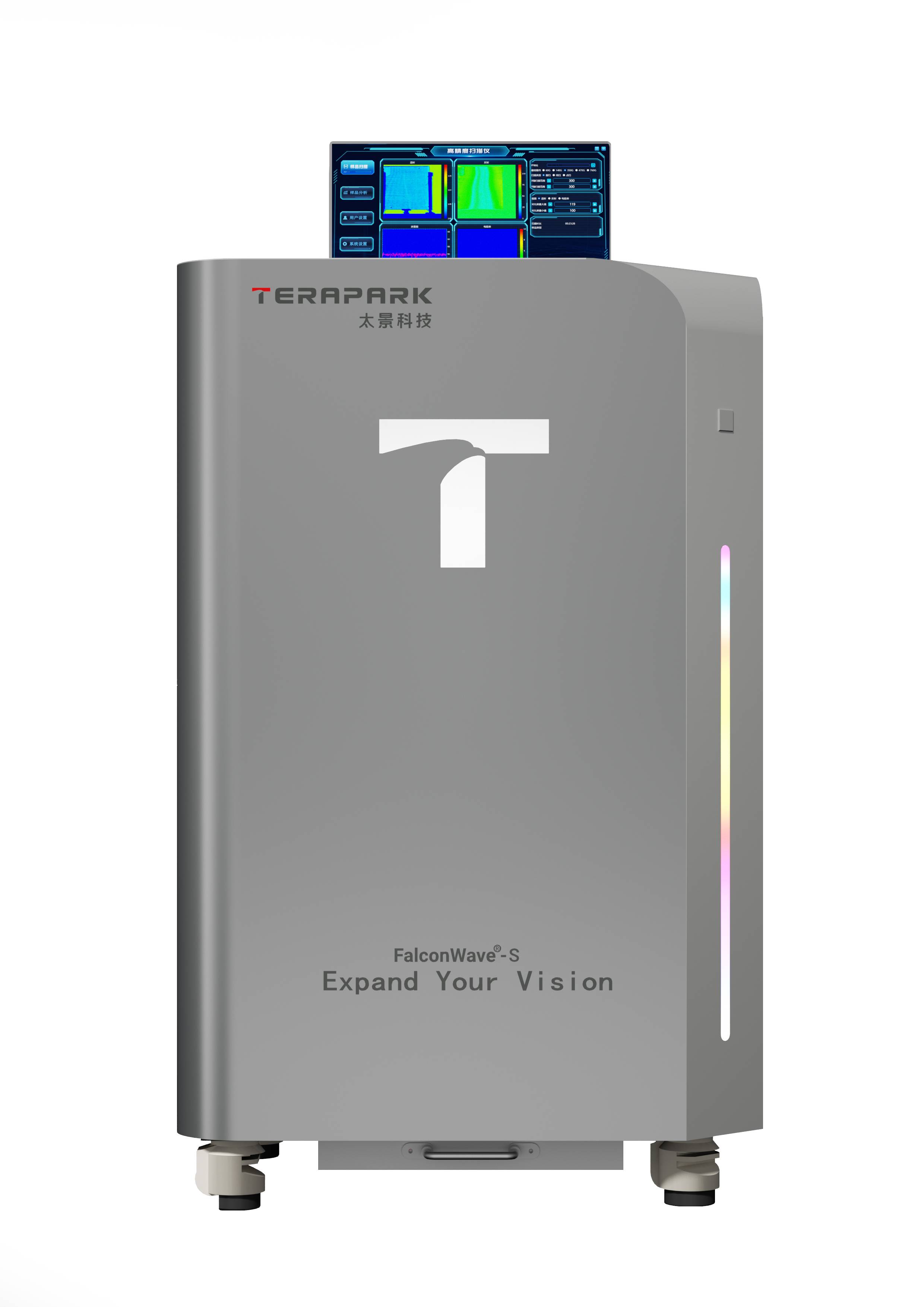
FalconWave®-S High Resolution Product
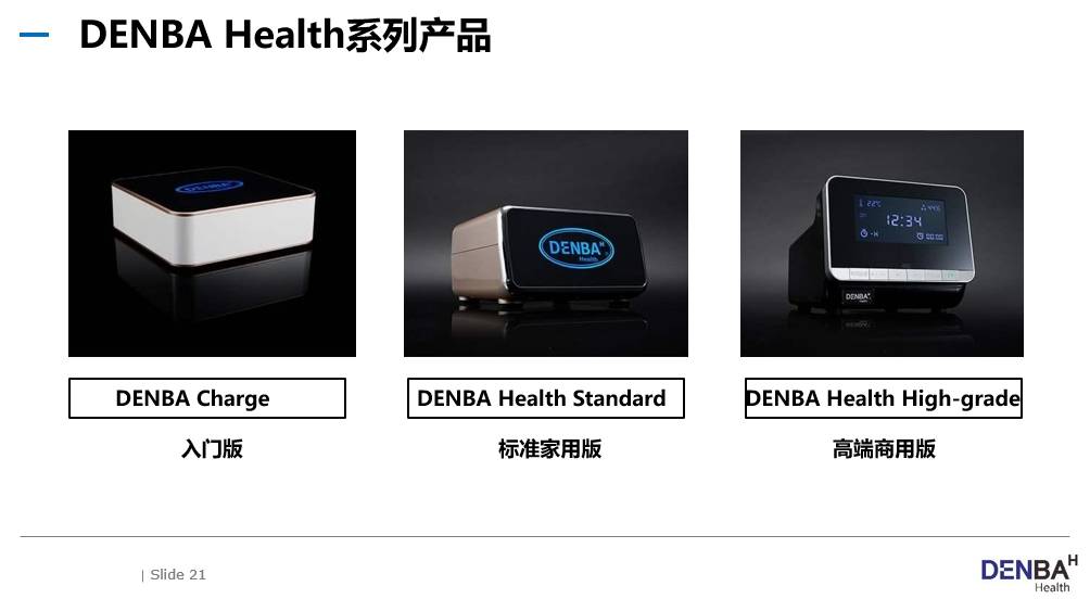
DENBA HEALTH
![[Used] laser](https://cdn.sumecdtx.com/equipment/20230818/928f9346aceb42e3b60670c380399f59.jpg)
[Used] laser
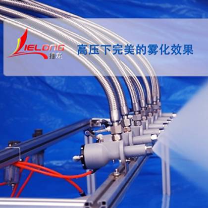
High pressure atomization and spraying system
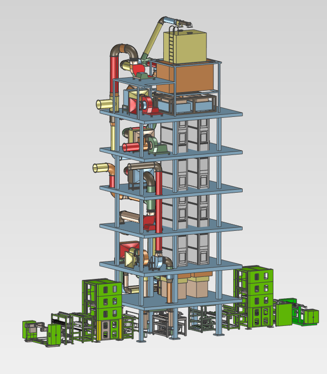
6/8 inch resistor long crystal furnace
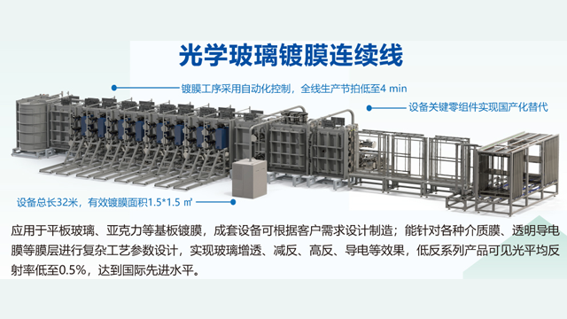
Optical anti-reflection coating continuous line
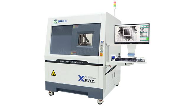
Electronic manufacturing of X-Ray inspection equipment
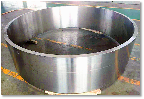
Titanium products、Copper alloy products
IR Vertical Impregnation Machine
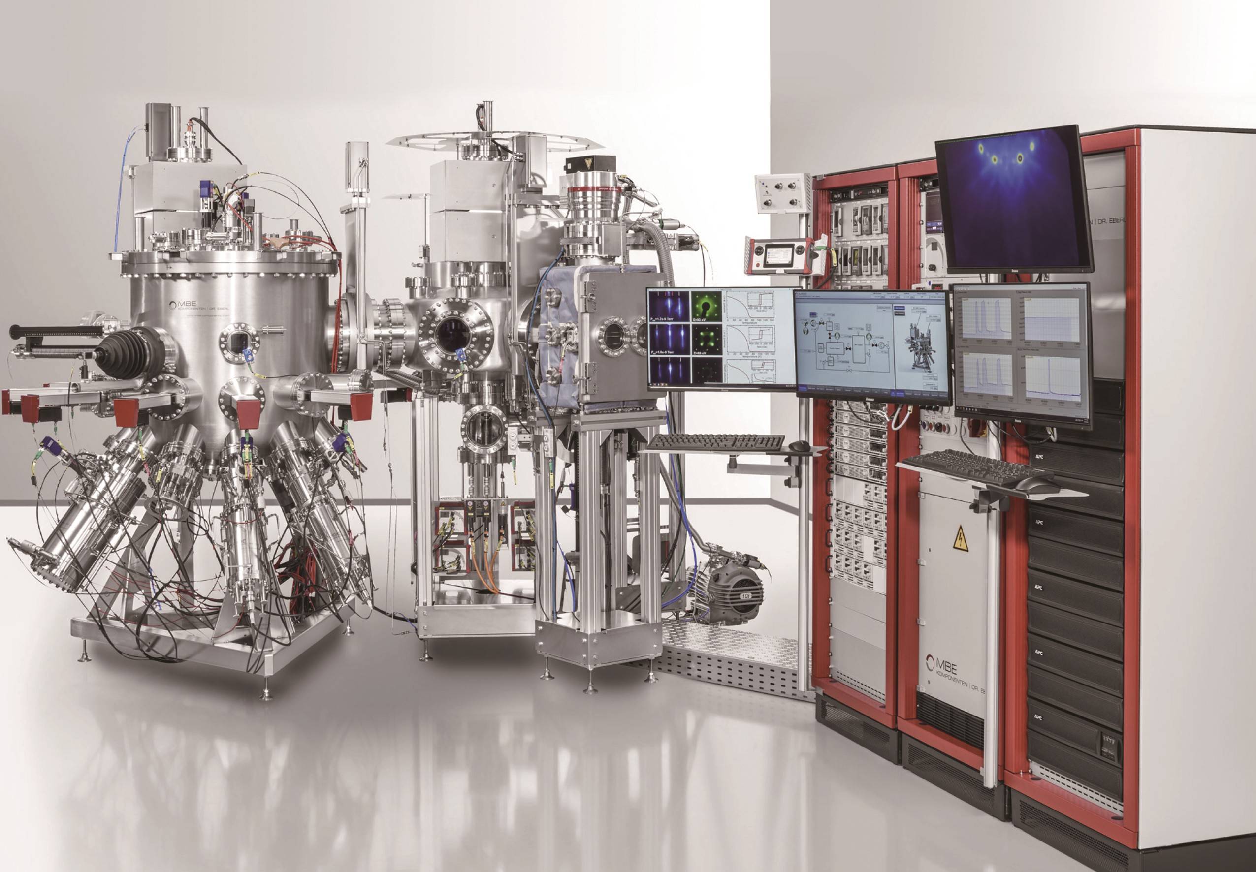
Molecular beam epitaxial system MBE