

 Search


 Post Requirements

 Post Requirements
Product information
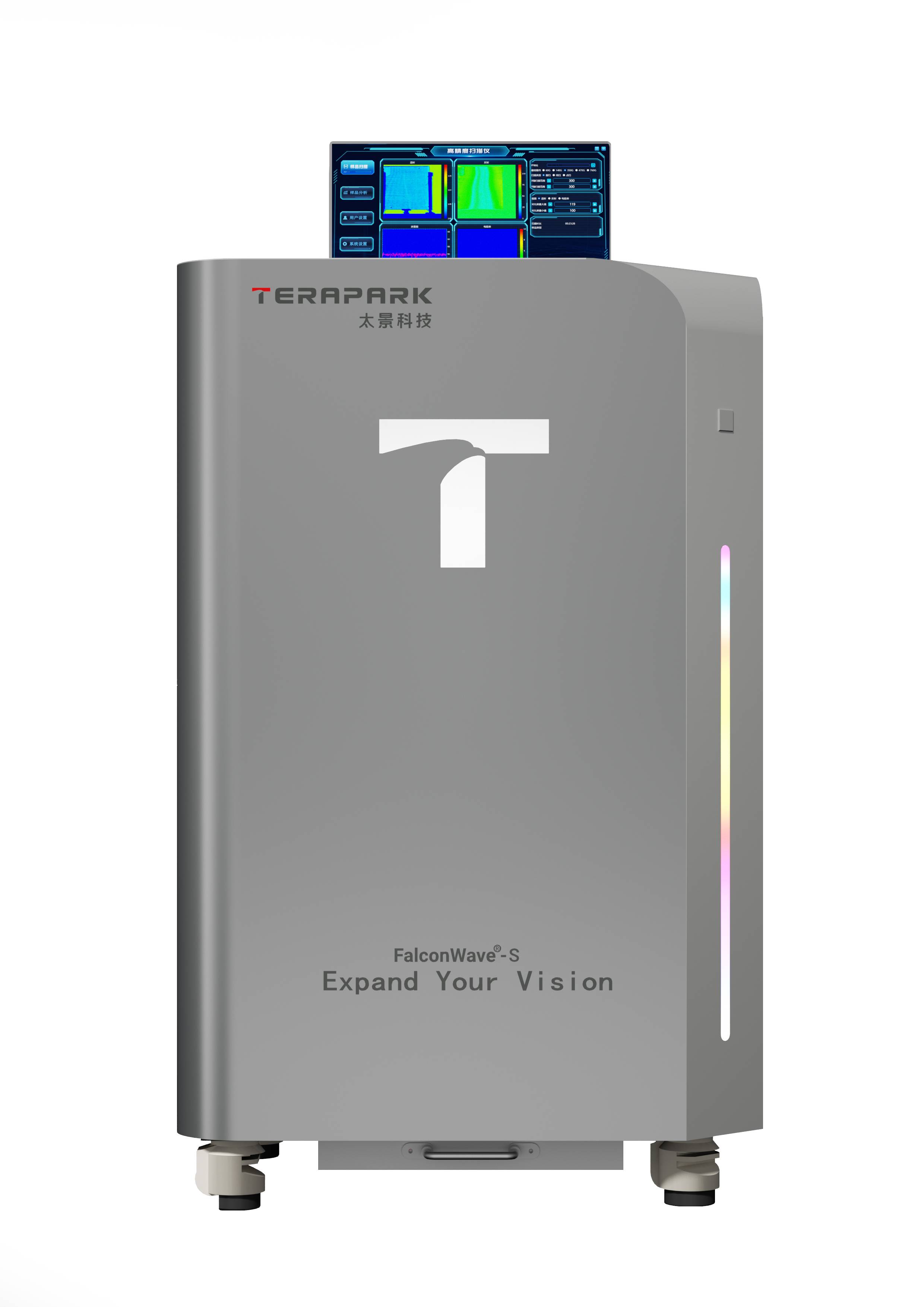
The patterned wafer defect inspection equipment has bright field, dark field, AI, and combined with spatial filtering technology, which can inspect defects such as particles, scratches, pits, and protrusions on patterned Si/GaN/SiC wafers. The main application of this tool is to inspect various front-end process nodes in HVM IC Fab, in order to improve the yield of chip production.
Equipment Description Features
Wafer handling EFEM: 6 "/8" SMIF or 12 "FOUP
Suitable for Si/GaN/SiC wafers
Wafer warpage not exceeding 200um
Wafer thickness 350um~1.5mm (bottom clamp)
Bright field and oblique dark field
Patterned wafer particle inspection sensitivity 100nm
Process Node 90-130nm
Options Available
/OCR: OCR, recognition rate ≥ 99% (compliant with SEMI font standards, except for unclear engraving)
/IV: Offline image viewing software that can be used for offline analysis
/SG: SECS-GEM, supports SEMI automation standard SECS/GEM communication interface, complies with SEMI E5- (SECS-II), SEMI E30- (GEM), SEMI E37- (HSMS) communication standards, and retains other communication protocol interfaces
/PSL: PSL Si standard wafer


![[Second-hand] laser](https://cdn.sumecdtx.com/equipment/20230818/928f9346aceb42e3b60670c380399f59.jpg)


