

 Search


 Quality partner
 Time of Registration : 2 Years
 industry experience : 6 YearsREG : 2 YearsEXP : 6 Years
 Post Requirements
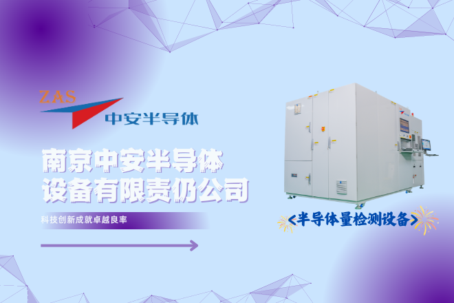
- 1
- 1
ZAS Semiconductor is a company established in 2020, headquartered in Jiangbei New District, Nanjing City. The company is dedicated to driving the development of the semiconductor inspection-related industry chain, including precision instruments, precision machinery, optical module processing, deep ultraviolet optical component processing, high-resolution cameras, and more.
Company establishment (2020.03) : ZAS Semiconductor was established in March 2020, headquartered in Jiangbei New District, Nanjing.
In October 2020, the geometric topography measurement equipment completed the 200mm principle verification machine.
In May 2021, the graphic geometry measurement equipment completed the 200mm/300mm transition model.
In June 2021, the 200mm prototype of the geometric topography measurement equipment was completed.
In August 2021, a 300mm prototype was completed by the geometric shape measurement equipment.
Product market expansion (2021.11-2022.12) :
In November 2021, the PCG project was launched to start the research and development of particle detection equipment.
In December 2021, the first domestic graphic geometry measurement equipment was shipped and entered the Fab client.
In April 2022, the non-graphic geometry measurement equipment obtained the first domestic silicon wafer factory order.
In July 2022, the graphics geometry measurement equipment completed the first full-wafer with graphics in China.
In September 2022, the geometric topography measurement equipment was delivered to the first domestic silicon wafer factory without graphic geometry.
In December 2022, the graphic geometry measurement equipment obtained batch orders from customers.
Product Innovation (2023.12) :
In December 2023, the prototype of particle detection equipment will be completed to further enhance the product line."
ZAS Semiconductor is a company established in 2020, headquartered in Jiangbei New District, Nanjing City. The company is dedicated to driving the development of the semiconductor inspection-related industry chain, including precision instruments, precision machinery, optical module processing, deep ultraviolet optical component processing, high-resolution cameras, and more.The core technology of the company is advanced patented technology in the field of measurement, as well as an autonomous and controllable supply chain system.
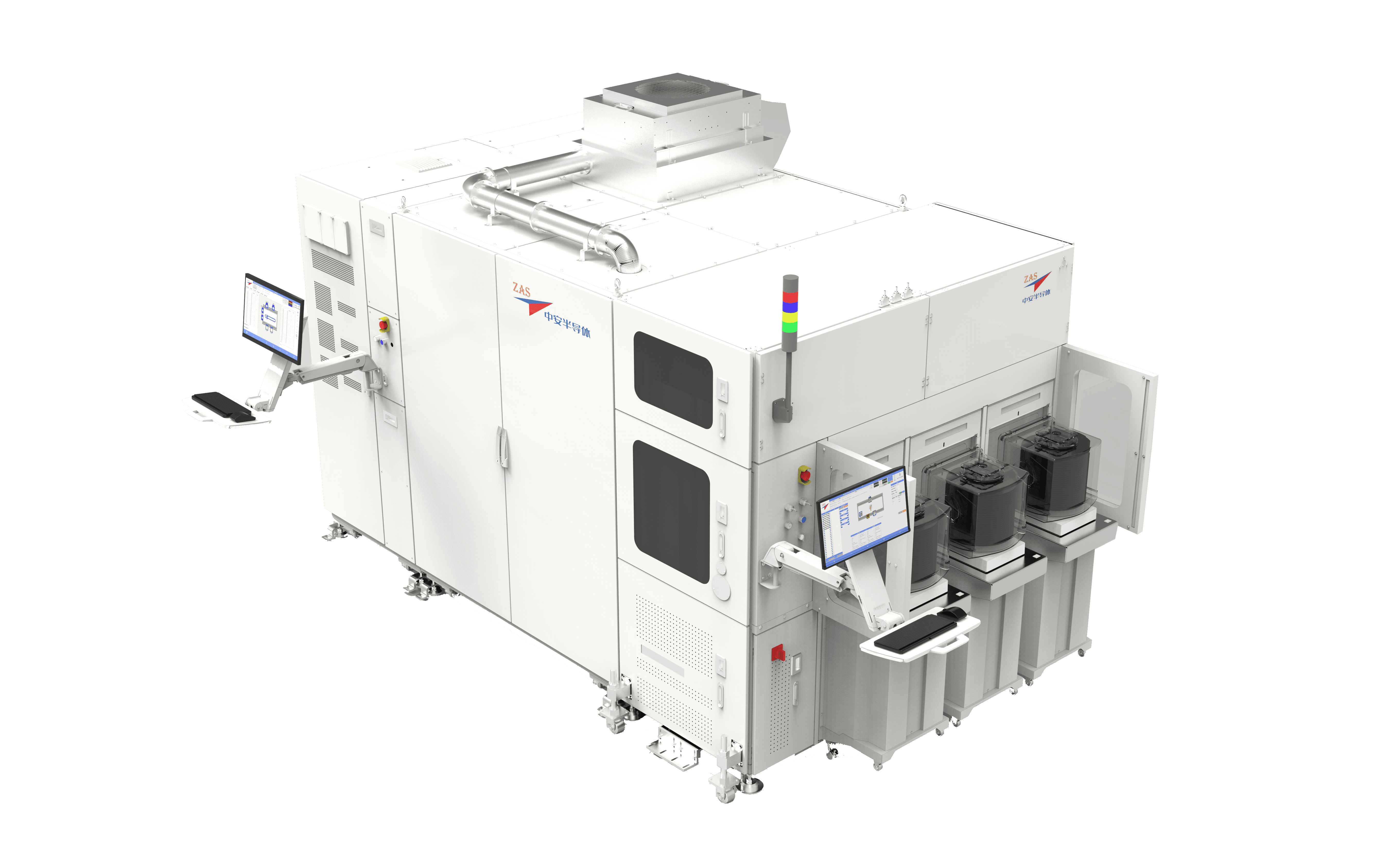
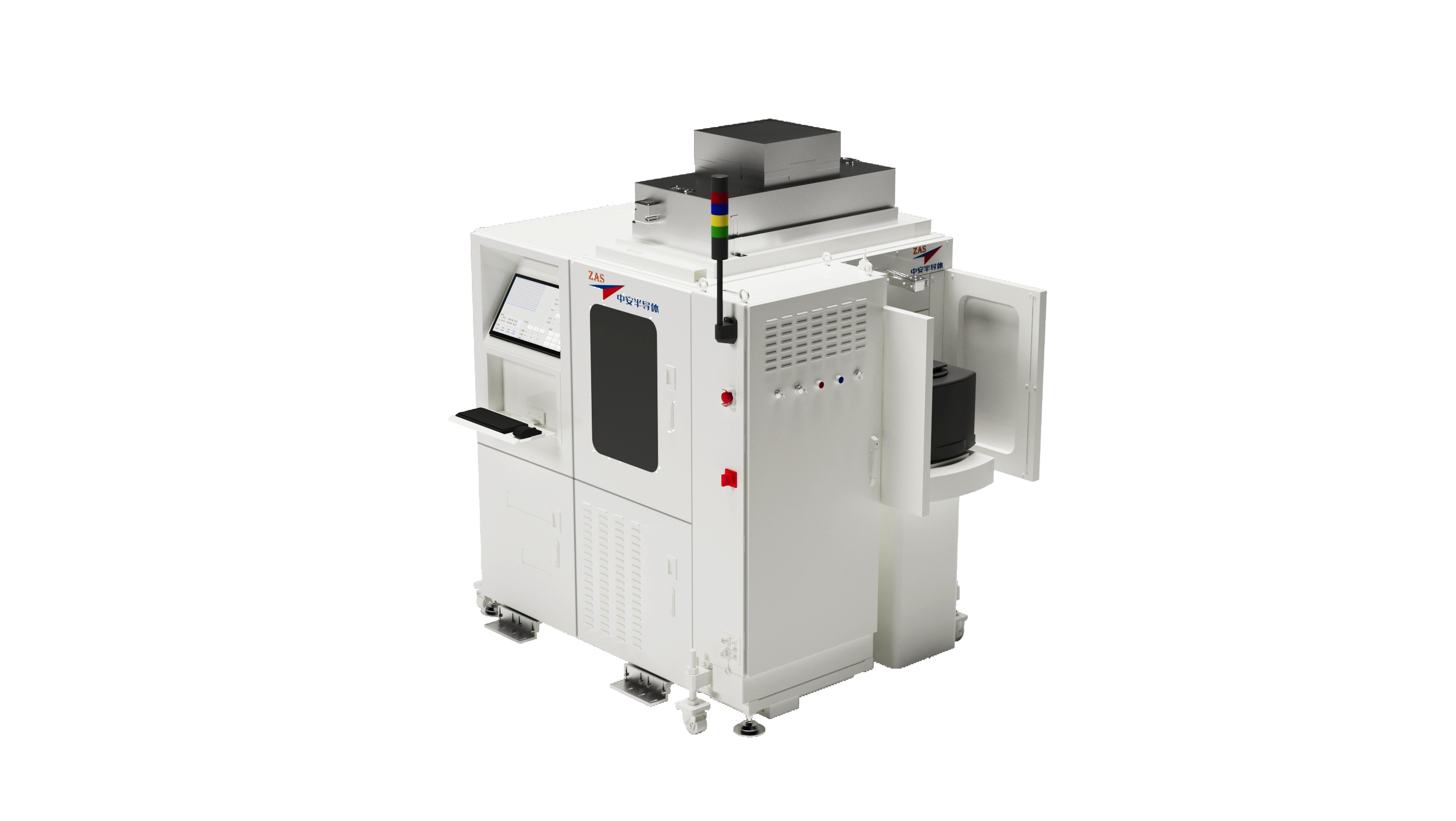
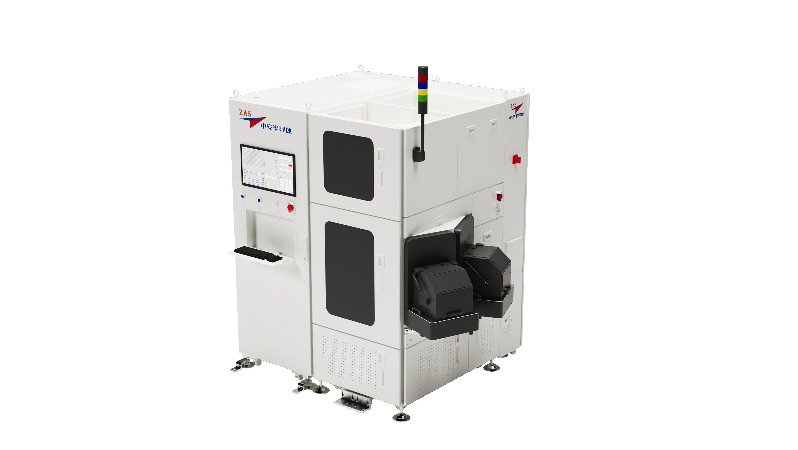
Since the establishment of the company, ZAS Semiconductor has continuously innovated, rapidly introduced a series of geometric shape measurement equipment and particle detection equipment, and made a series of important progress. The company's geometry measurement equipment plays a key role in the wafer manufacturing process, providing key parameters such as stress, warpage and flatness. Compared with traditional products, ZAS Semiconductor‘s equipment has the advantages of high precision, rapid testing and high data density, which is highly recognized by customers and supported by batch orders.
At the same time, ZAS Semiconductor also focuses on the development of non-graphic wafer particle detection equipment, which can quickly detect particles, scratches and other defects on the wafer surface, meeting the needs of mature processes and high-level needs.
With advanced technology and excellent products, ZAS Semiconductor has won investment and support from domestic and foreign investment institutions and industry capital, providing strong support for the company's research and development and production and operation."