Established in 2017, headquartered in Beijing, AK Optics has research and development and production bases in Beijing, Hangzhou, and Nanchang. The company was founded by senior overseas experts and is an enterprise that integrates research and development, production, sales, and service.
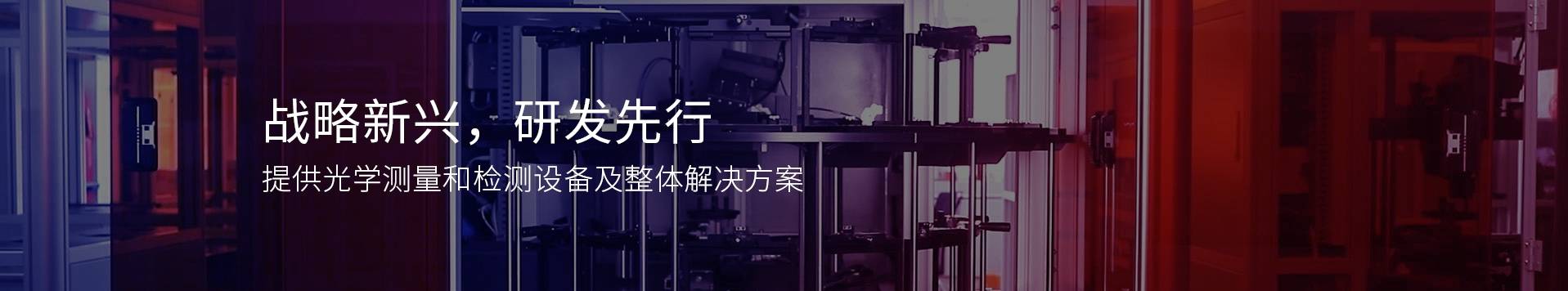
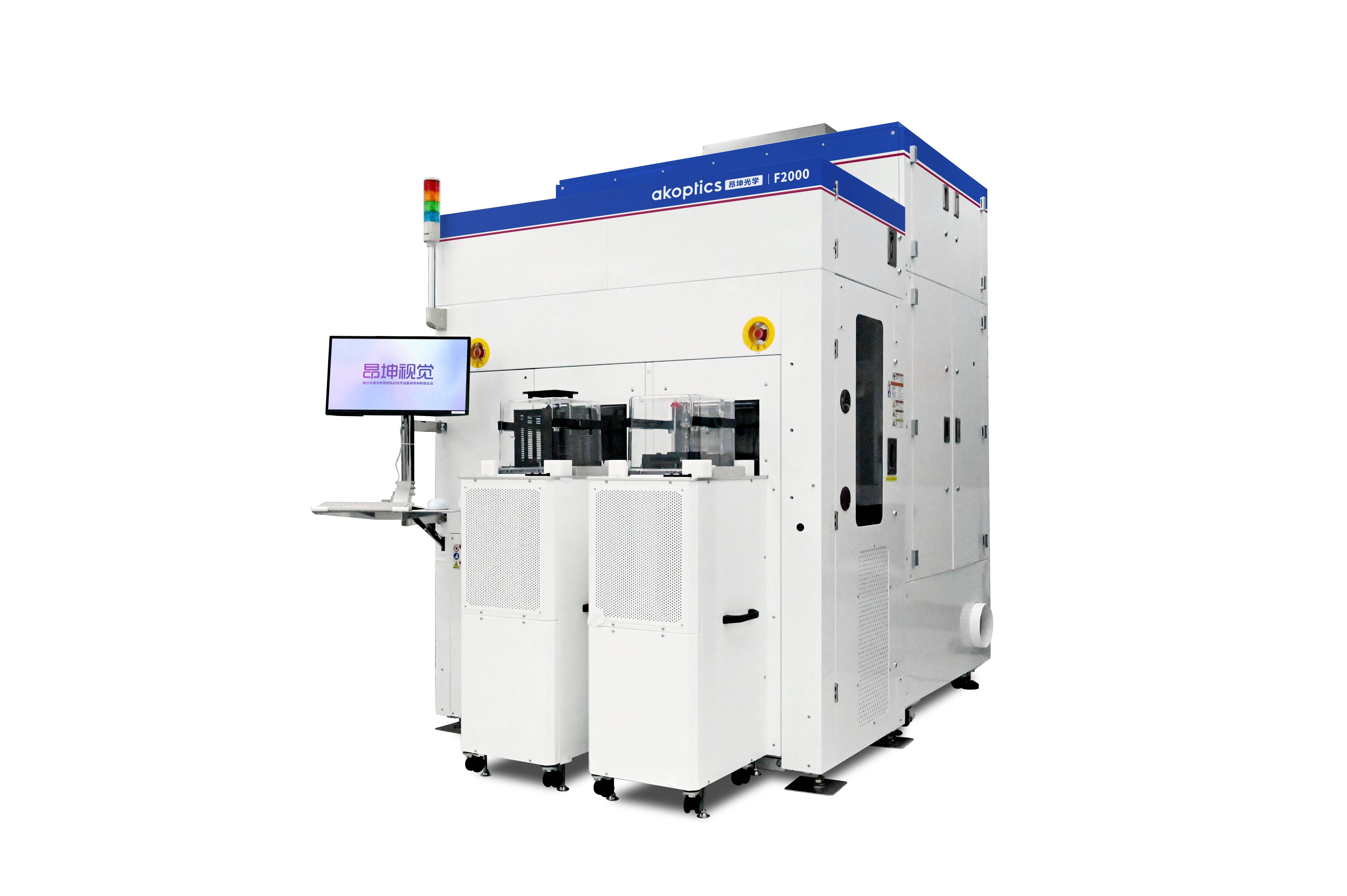
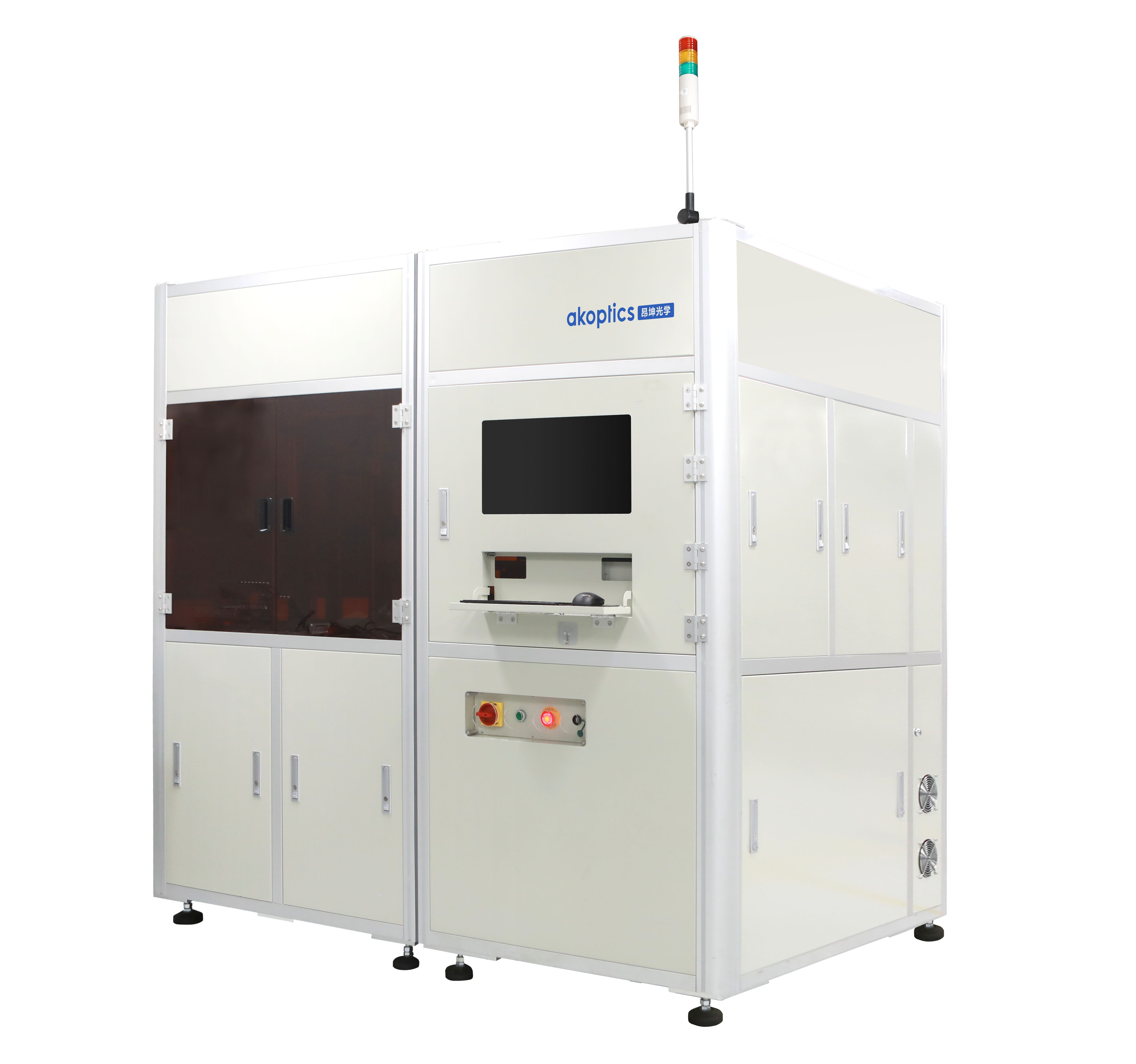
Focused on providing optical measurement and inspection equipment and solutions for the compound semiconductor, optoelectronic, and integrated circuit industries. Its products cover multiple aspects of production process measurement and testing in related industries, including substrate thickness and morphology measurement, substrate particle inspection, epitaxial wafer inspection, chip appearance inspection, MOCVD online monitoring, etc
Adhering to independent originality, we have accumulated and made breakthroughs in key technologies such as optical system design, optical imaging technology, and AI algorithms. We have multiple leading technologies independently developed and possess industry recognized research and development capabilities.
The company's series of wafer defect inspection equipment has been mass-produced in the fields of LED chips, compound semiconductors, and specialty process integrated circuits, and has gained market recognition.
Obtained recognition as a national high-tech enterprise, Zhongguancun high-tech enterprise, specialized and innovative small and medium-sized enterprise, and specialized and innovative "little giant" enterprise


 Search


 Time of Registration : 1 Years
 industry experience : 9 Years
 Post Requirements